MPC5553/MPC5554 Microcontroller Reference Manual, Rev. 5
Freescale Semiconductor 13-7
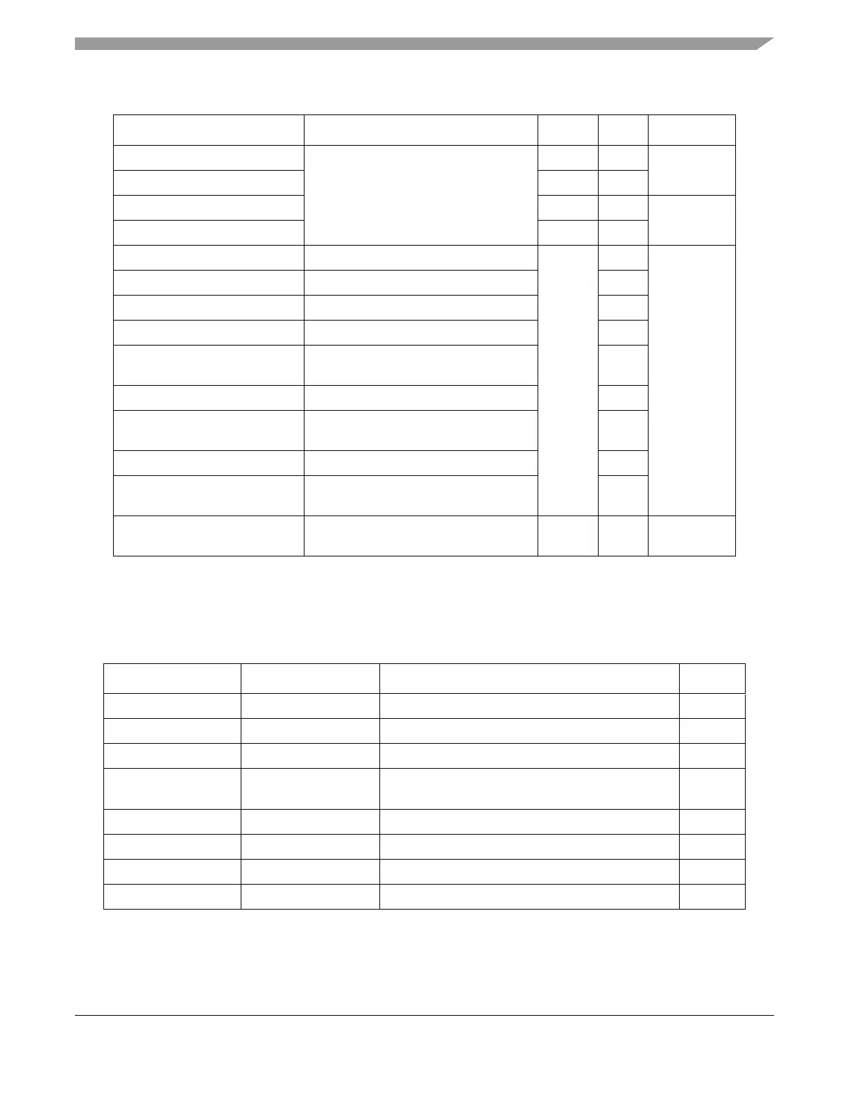
Table 13-5 shows the register set for the flash module.
Array Base + 0x18_0000 High-address space (MPC5554 only) H8
1
128K 8
1
Array Base + 0x1A_0000 H9
1
128K
Array Base + 0x1C_0000 H10
1
128K 9
1
Array Base + 0x1E_0000 H11
1
128K
Array Base + 0xFF_FC00 Shadow block space S 472 All
2
Array Base+ 0xFF_FDD8 Flash shadow row, serial passcode 8
Array Base+ 0xFF_FDE0 Flash shadow row, control word 4
Array Base+ 0xFF_FDE4 For general use 4
Array Base+ 0xFF_FDE8 Flash shadow row, FLASH_LMLR
reset configuration
4
Array Base+ 0xFF_FDEC For general use 4
Array Base+ 0xFF_FDF0 Flash shadow row, FLASH_HLR
reset configuration
4
Array Base+ 0xFF_FDF4 For general use 4
Array Base+ 0xFF_FDF8 Flash shadow row, FLASH_SLMLR
reset configuration
4
Array Base+
0xFF_FDFC – 0xFF_FFFF
For general use 516
1
Not available in the MPC5553; only available in the MPC5554.
2
The shadow row does not support RWW. See Section 13.4.2.5, “Flash Shadow Block.
Table 13-5. Module Register Memory Map
Byte Address Register Name Register Description Size (bits)
Register Base+0x0000 FLASH_MCR Module configuration register 32
Register Base+0x0004 FLASH_LMLR Low-/mid-address space block locking register 32
Register Base+0x0008 FLASH_HLR High-address space block locking register 32
Register Base+0x000C FLASH_SLMLR Secondary low-/mid-address space block
locking register
32
Register Base+0x0010 FLASH_LMSR Low-/mid-address space block select register 32
Register Base+0x0014 FLASH_HSR High-address space block select register 32
Register Base+0x0018 FLASH_AR Address register 32
Register Base+0x001C FLASH_BIUCR Flash bus interface unit control register 32
Table 13-4. Flash Partitions (Continued)
Address Use Block Size Partition