MPC5553/MPC5554 Microcontroller Reference Manual, Rev. 5
Freescale Semiconductor 18-13
18.3.2.2 Time Base Clock Signal (TCRCLK[A:B])
The TCRCLK[A:B] input signals are used to control the TCR1 and TCR2 time bases for eTPU A and
eTPU B.
NOTE
Throughout this document, TCRCLKA and TCRCLKB are referred to
generically as TCRCLK.
There is one independent TCRCLK input for each engine. Table 18-3 shows the TCRCLK pin
connections. For pulse accumulator operations TCRCLK can be used as a gate for a counter based on the
system clock divided by eight. For angle operations TCRCLK can be used to get the tooth transition
indications in angle mode. Further details can be found in the eTPU reference manual’s Section 5.9 and
5.10.
18.3.2.3 Channel Output Disable Signals
Each eTPU engine has four input signals that are used to force the outputs of a group of 8 channels to an
inactive level. These signals originate from the eMIOS. When an output disable signal is active, all the 8
channels assigned to the disable signal that have their ODIS bits set to 1 in ETPU_CnCR register have their
outputs forced to the opposite of the value specified in the ETPU_CnCR[OPOL] bit. Therefore, individual
channels can be selected to be affected by the output disable signals, as well as their disabling forced
polarity. Refer to Section 17.2.1.2, “Output Disable Input—eMIOS Output Disable Input Signals for more
information on the output disable signals.
8–15 I K24, J26, K23, J25,
J24, H26, H25, G26
8–15 not connected eTPU_B[8:15] eTPU_B[24:31]
(output only)
GPIO[155:162]
O DSPI_A[7:0]
1
16–31 I D16, D17, A17, C16,
A18, B17, C17, D18,
A19, B18, C18, A20,
B19, D19, C19, B20
16–31 not connected eTPU_B[16:31] GPIO[163:178]
O
1
The channel numbers for some of the DSPI channels connections are reversed, for example if eTPU_B[0:7] is mapped
to DSPI_A[15:8], then eTPU_B[0] is connected to DSPI_A[15], eTPU_B[1] is connected to DSPI_A[14],..., eTPU_B[7] is
connected to DSPI_A[8].
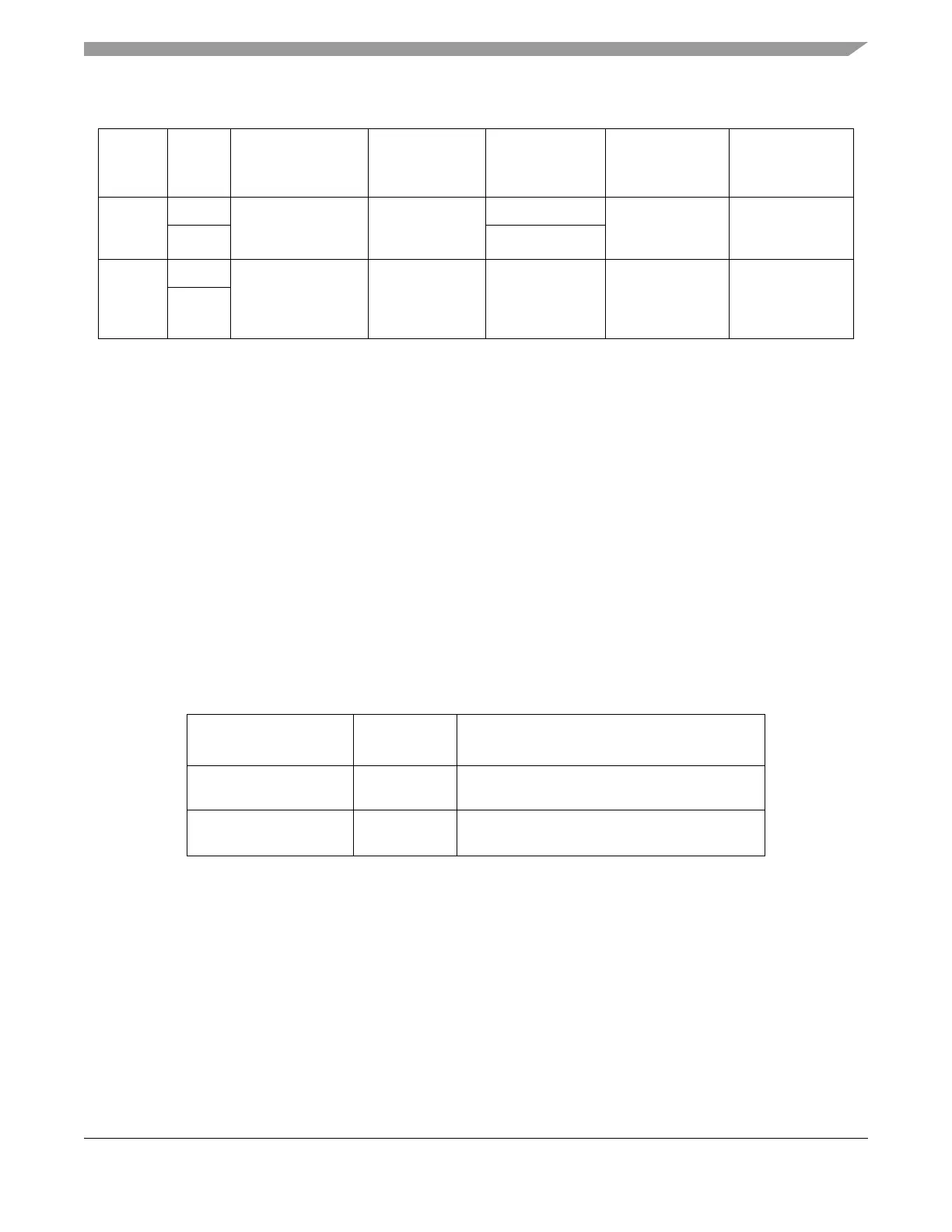
Table 18-3. TCRCLK Signals
Signal Name
Pin
Connection
Other Signals Muxed on Same Pin
TCRCLKA N4 IRQ7 (input only)
GPIO113
TCRCLKB
1
1
TCRCLKB is implemented only in the MPC5554.
M23 IRQ6 (input only)
GPIO146
Table 18-2. eTPU B Channel Connection Table (MPC5554 Only) (Continued)
eTPU
Channel
Number
I/O Pin Number
eTPU Channel
Connections
DSPI Serial
Channel
Connections
eTPU B
Signal
Signals with
Which eTPU
Signal is Shared: