MPC5553/MPC5554 Microcontroller Reference Manual, Rev. 5
Freescale Semiconductor 19-41
NOTE
If TBC_CLK_PS is not set to disabled, it must not be changed to any other
value besides disabled. If TBC_CLK_PS is set to disabled it can be changed
to any other value.
19.3.3.3 ADC Time Base Counter Registers (ADC_TBCR)
The ADC_TBCR contains the current value of the time base counter. ADC_TBCR can be accessed by
configuration commands sent to ADC0 or to ADC1. A data write to ADC_TBCR through a configuration
command sent to ADC0 will write the same memory location as when writing to it through a configuration
command sent to ADC1.
NOTE
Simultaneous write accesses from ADC0 and ADC1 to ADC_TBCR are not
allowed.
0b1011 128 0.94
0b1100 256 0.47
0b1101 512 0.23
0b1110 - 0b1111 Reserved —
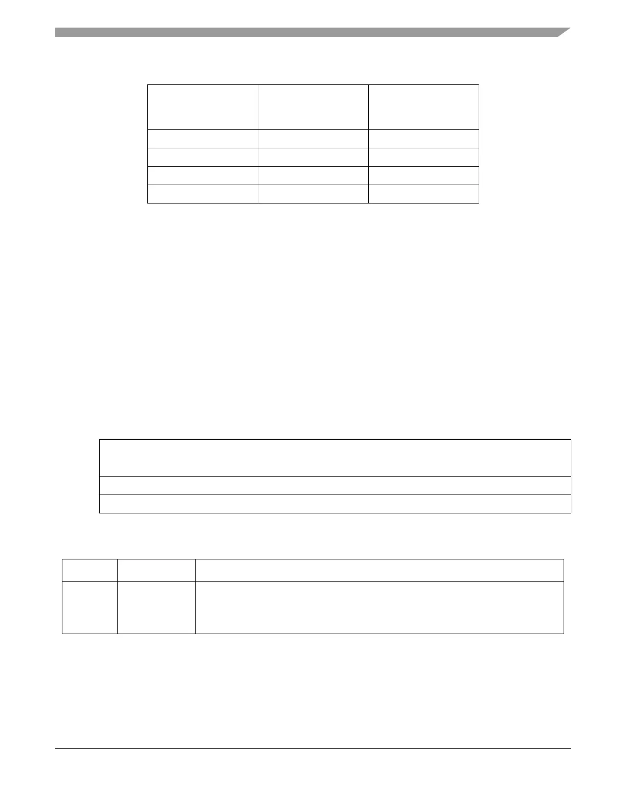
0123456789101112131415
R TBC_VALUE
W
Reset0000000000000000
Reg Addr 0x03
Figure 19-21. ADC Time Base Counter Register (ADC_TBCR)
Table 19-31. ADC_TBCR Field Descriptions
Bits Name Description
0–15 TBC_VALUE
[0:15]
Time base counter VALUE. Contains the current value of the time base counter. Reading
TBC_VALUE returns the current value of time base counter. Writes to TBC_VALUE
register load the written data to the counter. The time base counter counts from 0x0000 to
0xFFFF and wraps when reaching 0xFFFF.
Table 19-30. Clock Divide Factor for Time Stamp (Continued)
TBC_CLK_PS[0:3]
System Clock Divide
Factor
Clock to Time Stamp
Counter for a 120 MHz
System Clock (MHz)