MPC5553/MPC5554 Microcontroller Reference Manual, Rev. 5
Freescale Semiconductor 20-53
DSPIx_CTARn registers select the PCS to SCK delay, and the relationship is expressed by the following
formula:
Table 20-24 shows an example of the computed PCS to SCK delay.
20.4.6.3 After SCK Delay (t
ASC
)
The after SCK delay is the length of time between the last edge of SCK and the negation of PCS. See
Figure 20-36 and Figure 20-37 for illustrations of the after SCK delay. The PASC and ASC fields in the
DSPIx_CTARn registers select the after SCK delay. The relationship between these variables is given in
the following formula:
Table 20-25 shows an example of the computed after SCK delay.
20.4.6.4 Delay after Transfer (t
DT
)
The delay after transfer is the length of time between negation of the PCS signal for a frame and the
assertion of the PCS signal for the next frame. See Figure 20-36 for an illustration of the delay after
transfer. The PDT and DT fields in the DSPIx_CTARn registers select the delay after transfer. The
following formula expresses the PDT/DT/delay after transfer relationship:
Table 20-26 shows an example of the computed delay after transfer.
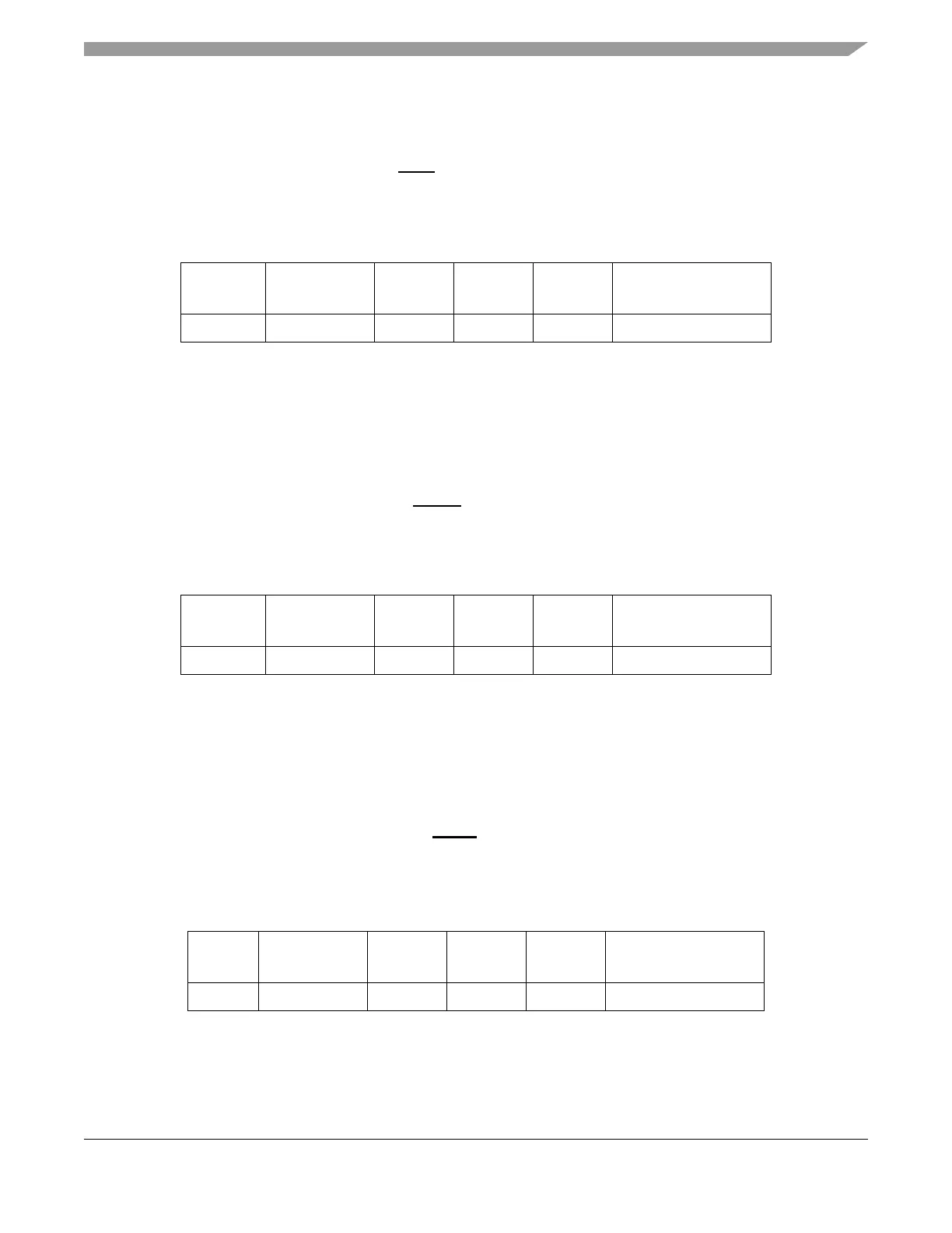
Table 20-24. PCS to SCK Delay Computation Example
PCSSCK
Prescaler
Value
CSSCK
Scaler
Value
f
SYS PCS to SCK Delay
0b01 3 0b0100 32 100 MHz 0.96 s
Table 20-25. After SCK Delay Computation Example
PASC
Prescaler
Value
ASC
Scaler
Value
Fsys After SCK Delay
0b01 3 0b0100 32 100 MHz 0.96 us
Table 20-26. Delay after Transfer Computation Example
PDT
Prescaler
Value
DT
Scaler
Value
f
SYS Delay after Transfer
0b01 3 0b1110 32768 100 MHz 0.98 ms
t
CSC
=
f
SYS
CSSCK
PCSSCK
1