MPC5553/MPC5554 Microcontroller Reference Manual, Rev. 5
20-58 Freescale Semiconductor
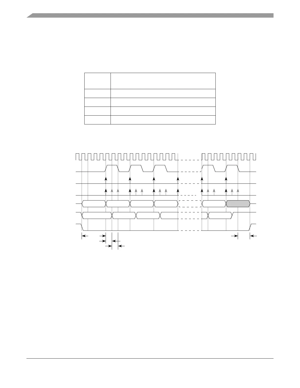
The master places its second data bit on the SOUT line one system clock after odd numbered SCK edge.
The point where the master samples the slave SOUT is selected by writing to the SMPL_PT field in the
DSPIx_MCR. Table 20-29 lists the number of system clock cycles between the active edge of SCK and
the master sample point for different values of the SMPL_PT bit field. The master sample point can be
delayed by one or two system clock cycles.
Figure 20-38 shows the modified transfer format for CPHA = 0. Only the condition where CPOL = 0 is
illustrated. The delayed master sample points are indicated with a lighter shaded arrow.
Figure 20-38. DSPI Modified Transfer Format (MTFE = 1, CPHA = 0, Fsck = Fsys/4)
20.4.7.4 Modified SPI/DSI Transfer Format (MTFE = 1, CPHA = 1)
Figure 20-39 shows the modified transfer format for CPHA = 1. Only the condition where CPOL = 0 is
described. At the start of a transfer the DSPI asserts the PCS signal to the slave device. After the PCS to
SCK delay has elapsed the master and the slave put data on their SOUT pins at the first edge of SCK. The
slave samples the master SOUT signal on the even numbered edges of SCK. The master samples the slave
SOUT signal on the odd numbered SCK edges starting with the 3rd SCK edge. The slave samples the last
bit on the last edge of the SCK. The master samples the last slave SOUT bit one half SCK cycle after the
last edge of SCK. No clock edge will be visible on the master SCK pin during the sampling of the last bit.
The SCK to PCS delay must be greater or equal to half of the SCK period.
Table 20-29. Delayed Master Sample Point
SMPL_PT
Number of System Clock Cycles between
Odd-numbered Edge of SCK and Sampling of SIN
00 0
01 1
10 2
11 Reserved
t
CSC
= PCS to SCK delay.
t
ASC
= After SCK delay.
System Clock
123456
PCS
t
ASC
SCK
Master Sample
Slave SOUT
Master SOUT
System Clock
System Clock
Slave Sample
t
CSC