MPC5553/MPC5554 Microcontroller Reference Manual, Rev. 5
20-60 Freescale Semiconductor
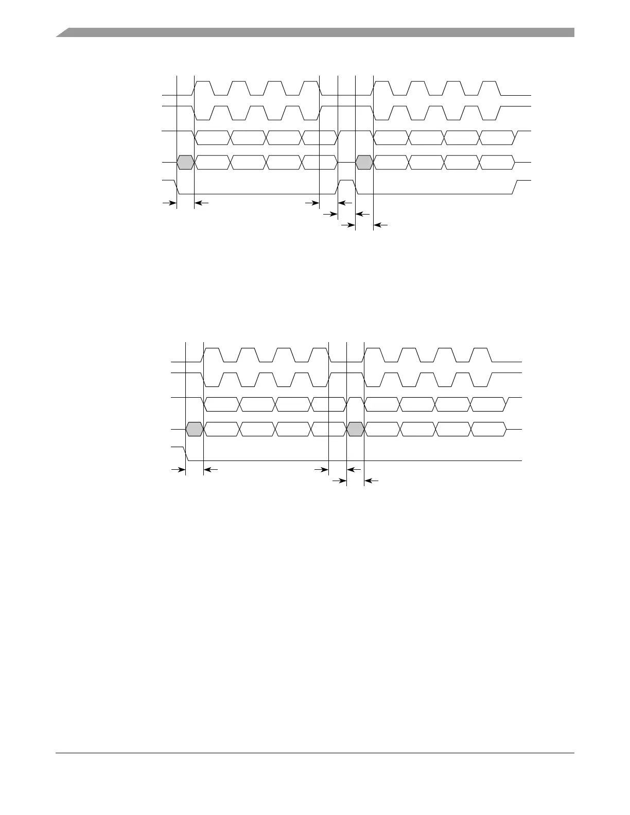
Figure 20-40. Example of Non-Continuous Format (CPHA=1, CONT=0)
When the CONT = 1 and the PCS signal for the next transfer is the same as for the current transfer, the
PCS signal remains asserted for the duration of the two transfers. The delay between transfers (t
DT
) is not
inserted between the transfers. Figure 20-41 shows the timing diagram for two four-bit transfers with
CPHA = 1 and CONT = 1.
Figure 20-41. Example of Continuous Transfer (CPHA = 1, CONT = 1)
In Figure 20-41, note that the period length at the start of the next transfer is the sum of t
ASC
and t
CSC
; i.e.,
it does not include a half-clock period. The default settings for these provide a total of four system clocks.
In many situations, t
ASC
and t
CSC
must be increased if a full half-clock period is required.
Switching CTARs between frames while using continuous selection can cause errors in the transfer. The
PCS signal must be negated before CTAR is switched.
When the CONT bit = 1 and the PCS signals for the next transfer are different from the present transfer,
the PCS signals behave as if the CONT bit was not set.
20.4.7.6 Clock Polarity Switching between DSPI Transfers
If it is desired to switch polarity between non-continuous DSPI frames, the edge generated by the change
in the idle state of the clock occurs one system clock before the assertion of the chip select for the next
frame. In Figure 20-42, time ‘A’ shows the one clock interval. Time ‘B’ is user programmable from a
SCK
(CPOL = 0)
PCSx
t
ASC
SCK
(CPOL = 1)
Master SOUT
t
DT
t
CSC
t
CSC
= PCS to SCK delay.
t
ASC
= After SCK delay.
t
DT
= Delay after transfer (minimum CS negation time).
Master SIN
t
CSC
SCK
(CPOL = 0)
PCS
t
ASC
SCK
(CPOL = 1)
Master SOUT
t
CSC
t
CSC
t
CSC
= PCS to SCK delay.
t
ASC
= After SCK delay.
Master SIN