MPC5553/MPC5554 Microcontroller Reference Manual, Rev. 5
21-12 Freescale Semiconductor
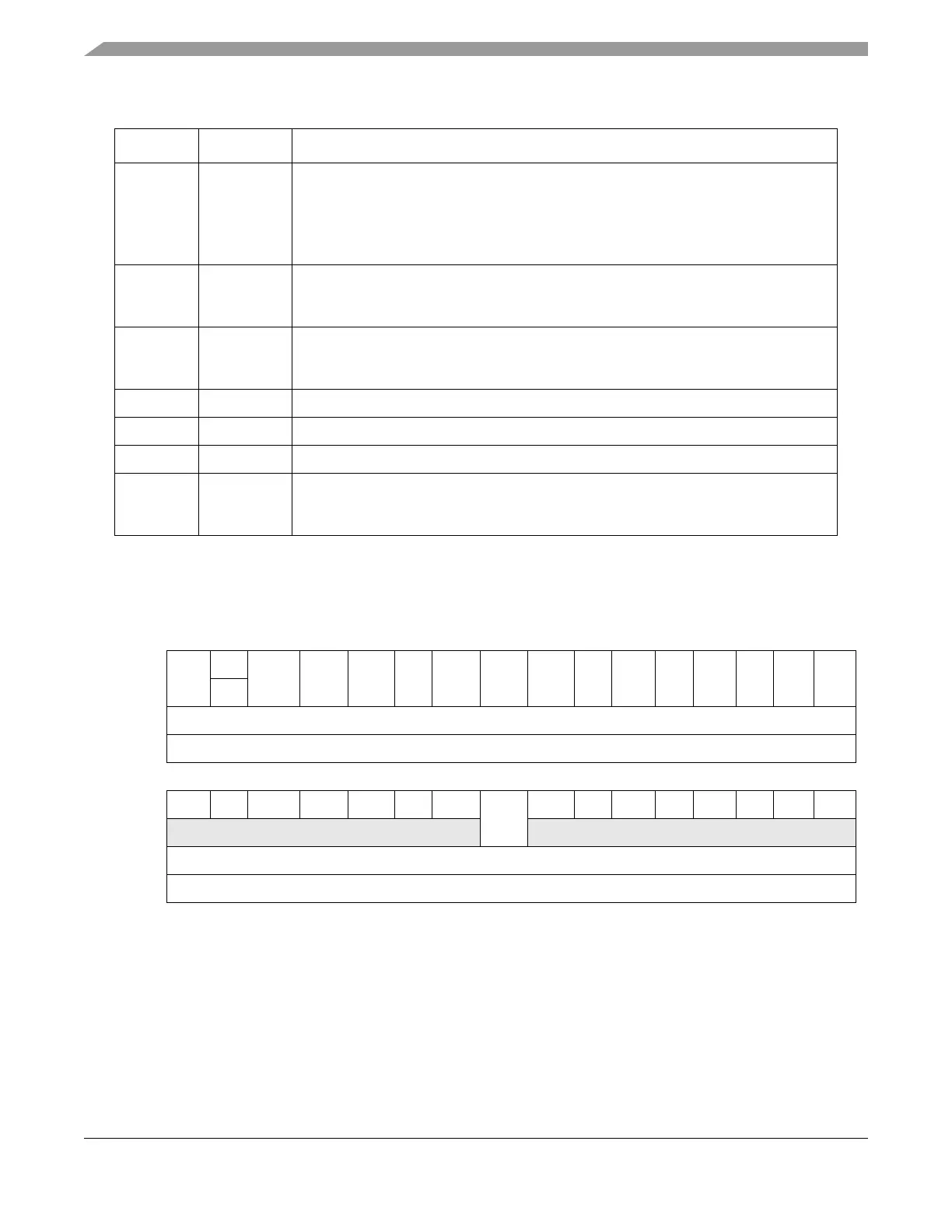
21.3.3.5 LIN Control Register (ESCIx_LCR)
ESCIx_LCR can be written only when there are no ongoing transmissions.
19 STO Slave time out. Represents a NO_RESPONSE_ERROR. This is set if a slave does not
complete a frame within the specified maximum frame length. For LIN 1.3 the following
formula is used:
20 PBERR Physical bus error. No valid message can be generated on the bus. This is set if, after
the start of a byte transmission, the input remains unchanged for 31 RT clock cycles.
This will reset the LIN FSM.
21 CERR CRC error. The CRC pattern received with an extended frame was not correct.
0 No error
1 CRC error
22 CKERR Checksum error. Checksum error on a received frame.
23 FRC Frame complete. LIN frame completely transmitted. All LIN data bytes received.
24–30 — Reserved.
31 OVFL ESCIx_LRR overflow. The LIN receive register has not been read before a new data
byte, CRC, or checksum byte has been received from the LIN bus. Set when the
condition is detected, and cleared by writing 1 to it.
0 1 2 3 4 5 6 7 8 9 10 11 12 13 14 15
R LRES 0 WUD0 WUD1 LDBG DSF PRTY LIN RXIE TXIE WUIE STIE PBIE CIE CKIE FCIE
WWU
Reset00 0 0 000 0 00000000
Reg Addr Base + 0x000C
16 17 18 19 20 21 22 23 24 25 26 27 28 29 30 31
R 0 0 0 0 0 0 0 OFIE 0 0 0 0 0 0 0 0
W
Reset00 0 0 000 0 00000000
Reg Addr Base + 0x000C
Figure 21-6. LIN Control Register (ESCIx_LCR)
Table 21-6. ESCIx_SR Field Descriptions (Continued)
Bits Name Description
TFRAME_MAX 10 NDATA 44+1.4=