MPC5553/MPC5554 Microcontroller Reference Manual, Rev. 5
25-58 Freescale Semiconductor
NOTE
For misaligned accesses (crossing 64-bit boundary), the access is broken
into two accesses. If both accesses are within the data trace range, two
DTMs will be sent: one with a size encoding indicating the size of the
original access (that is, word), and one with a size encoding for the portion
which crossed the boundary (that is, 3-byte).
NOTE
An STM to the cache’s store buffer within the data trace range will initiate
a DTM message. If the corresponding memory access causes an error, a
checkstop condition will occur. The debug/development tool should use this
indication to invalidate the previous DTM.
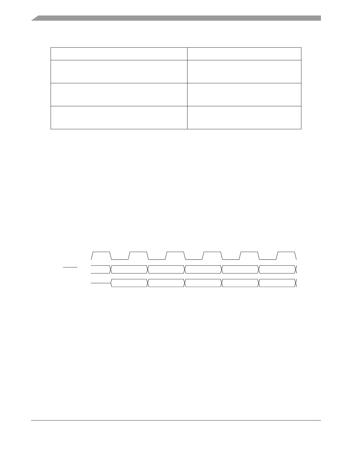
25.11.13.4 Data Trace Timing Diagrams (8 MDO Configuration)
Figure 25-45. Data Trace—Data Write Message
e200z6 bus cycle accesses misaligned data (across 64-bit
boundary)—both 1st & 2nd transactions within data trace
range
1st & 2nd cycle captured & 2 DTM’s transmitted
(see Note)
e200z6 bus cycle accesses misaligned data (across 64-bit
boundary)—1st transaction within data trace range; 2nd
transaction out of data trace range
1st cycle captured and transmitted; 2nd cycle
ignored
e200z6 bus cycle accesses misaligned data (across 64-bit
boundary)—1st transaction out of data trace range; 2nd
transaction within data trace range
1st cycle ignored; 2nd cycle capture and
transmitted
Table 25-37. e200z6 Bus Cycle Cases (Continued)
Special Case Action
MCKO
MSEO
[1:0]
TCODE = 5
Source Processor = 0b0000
Data Size = 010 (Half-Word)
Relative Address = 0xA5
00
MDO[7:0]
11 00 01 00 11
00000101 10101000 00010100 11101111 10111110
Write Data = 0xBEEF
 Loading...