MPC5553/MPC5554 Microcontroller Reference Manual, Rev. 5
25-78 Freescale Semiconductor
NOTE
DTSA must be less than (or equal to) DTEA in order to guarantee correct
data write/read traces. When the range control bit is 0 (internal range),
accesses to DTSA and DTEA addresses will be traced. When the range
control bit is 1 (external range), accesses to DTSA and DTEA will not be
traced.
25.14.2.6 Breakpoint / Watchpoint Control Register 1 (BWC1)
Breakpoint/watchpoint control register 1 controls attributes for generation of NXDM Watchpoint#1.
Table 25-50. Data Trace - Address Range Options
Programmed Values Range Control Bit Value Range Selected
DTSA < or = DTEA 0 DTSA-> <-DTEA
DTSA < or = DTEA 1 <- DTSA DTEA ->
DTSA > DTEA N/A Invalid range, no trace
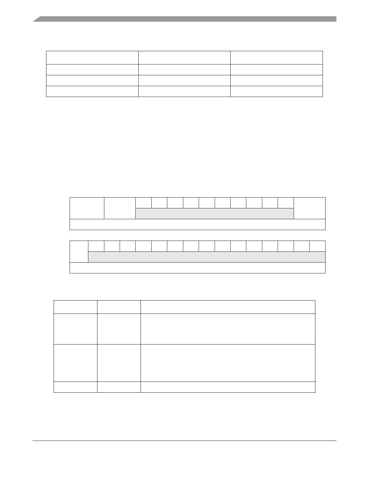
31 30 29 28 27 26 25 24 23 22 21 20 19 18 17 16
RBWE1 BRW1 0000000000 BWR1
W
Reset0 000000000000000
1514131211109876543210
RBWT1000000000000000
W
Reset0 000000000000000
Figure 25-59. Break / Watchpoint Control Register 1 (BWC1)
Table 25-51. BWC1 Field Description
Bit Name Description
31–30 BWE1 Breakpoint/watchpoint #1 enable
00 Internal Nexus watchpoint #1 disabled
01-10 Reserved
11 Internal Nexus watchpoint #1 enabled
29–28 BRW1 Breakpoint/watchpoint #1 read/write select
00 Watchpoint #1 hit on read accesses
01 Watchpoint #1 hit on write accesses
10 Watchpoint #1 on read or write accesses
11 Reserved
27–18 – Reserved, read as 0.