MPC5553/MPC5554 Microcontroller Reference Manual, Rev. 5
12-18 Freescale Semiconductor
0123456789101112131415
R001 BA
W
Reset00100000000 0 0000
Reg
Addr
Base + 0x0010 (EBI_BR0); Base + 0x0018 (EBI_BR1); Base + 0x0020 (EBI_BR2); Base + 0x0028 (EBI_BR3);
Base + 0x0040 (EBI_CAL_BR0); Base + 0x0048 (EBI_CAL_BR1); Base + 0x0050 (EBI_CAL_BR2); Base + 0x0058
(EBI_CAL_BR3)
16 17 18 19 20 21 22 23 24 25 26 27 28 29 30 31
RBA000PS0000BLWEBSTBDIP00BIV
W
Reset00000000000 0 0010
Reg
Addr
Base + 0x0010 (EBI_BR0); Base + 0x0018 (EBI_BR1); Base + 0x0020 (EBI_BR2); Base + 0x0028 (EBI_BR3);
Base + 0x0040 (EBI_CAL_BR0); Base + 0x0048 (EBI_CAL_BR1); Base + 0x0050 (EBI_CAL_BR2); Base + 0x0058
(EBI_CAL_BR3)
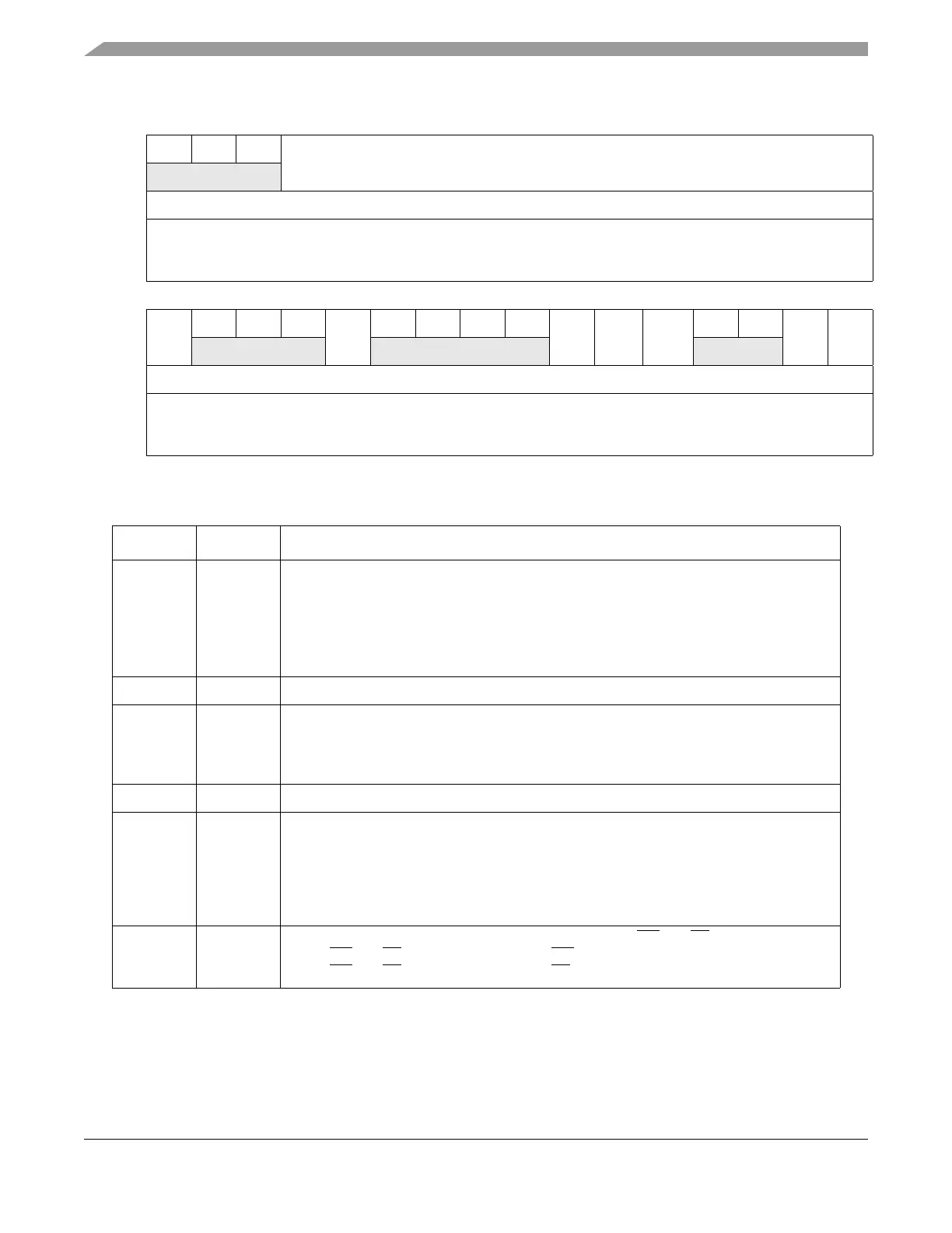
Figure 12-5. EBI Base Registers 0–3 (EBI_BRn) and EBI Calibration Base Registers 0–3 (EBI_CAL_BRn)
Table 12-10. EBI_BRn and EBI_CAL_BRn Field Descriptions
Bits Name Description
0–16 BA
[0:16]
Base address. Compared to the corresponding unmasked address signals among
ADDR[0:16] of the internal address bus to determine if a memory bank controlled by the
memory controller is being accessed by an internal bus master.
Note: The upper 3 bits of the base address (BA) field, EBI_BRn[0:2], and
EBI_CAL_BRn[0:2], are tied to a fixed value of 001. These bits reset to their fixed value.
17–19 — Reserved.
20 PS Port size. Determines the data bus width of transactions to this chip select bank.
1
0 32-bit port
1 16-bit port
Note: The calibration port size must be 16-bits wide.
21–24 — Reserved.
25 BL Burst length. Determines the amount of data transferred in a burst for this chip select,
measured in 32-bit words. The number of beats in a burst is automatically determined by
the EBI to be 4, 8, or 16 according to the port size so that the burst fetches the number of
words chosen by BL.
0 8-word burst length
1 4-word burst length
26 WEBS Write enable/byte select. Controls the functionality of the WE
[0:3]/BE[0:3] signals.
0The WE
[0:3]/BE[0:3] signals function as WE[0:3].
1The WE[0:3]/BE[0:3] signals function as BE[0:3].