MPC5553/MPC5554 Microcontroller Reference Manual, Rev. 5
Freescale Semiconductor 12-19
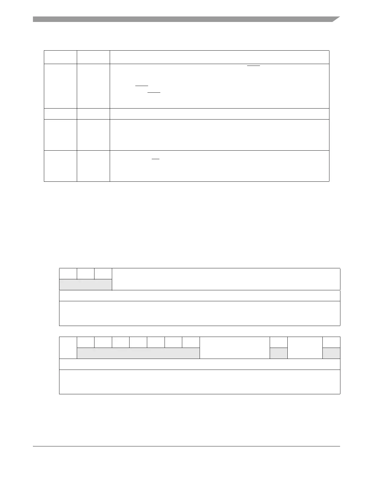
12.3.1.7 EBI Option Registers 0–3 (EBI_ORn) and EBI Calibration Option
Registers 0-3 (EBI_CAL_ORn)
The EBI_ORn registers are used to define the address mask and other attributes for the corresponding chip
select. The EBI_CAL_ORn registers appear in the MPC5553 only and are used to define the address mask
and other attributes for the corresponding calibration chip select.
27 TBDIP Toggle burst data in progress. Determines how long the BDIP signal is asserted for each
data beat in a burst cycle. See Section 12.4.2.5.1, “TBDIP Effect on Burst Transfer,” for
details.
0 Assert BDIP
throughout the burst cycle, regardless of wait state configuration.
1 Only assert BDIP
(BSCY + 1) external bus cycles before expecting subsequent burst
data beats.
28–29 — Reserved.
30 BI Burst inhibit. Determines whether or not burst read accesses are allowed for this chip
select bank.
0 Enable burst accesses for this bank.
1 Disable burst accesses for this bank. This is the default value out of reset.
31 V Valid bit. Indicates that the contents of this base register and option register pair are valid.
The appropriate CS
signal does not assert unless the corresponding V-bit is set.
0 This bank is not valid.
1 This bank is valid.
1
In the case where EBI_MCR[DBM] is set for 16-bit data bus mode, the PS bit value is ignored and is always treated
as a 1 (16-bit port).
0123456789101112131415
R111 AM
W
Reset1110000000000000
Reg Addr Base + 0x0014 (EBI_OR0); Base + 0x001C (EBI_OR1); Base + 0x0024 (EBI_OR2); Base + 0x002C (EBI_OR3);
Base + 0x0044 (EBI_CAL_OR0); Base + 0x004C (EBI_CAL_OR1); Base + 0x0054 (EBI_CAL_OR2); Base +
0x005C (EBI_CAL_OR3)
16 17 18 19 20 21 22 23 24 25 26 27 28 29 30 31
RAM0000000 SCY 0 BSCY 0
W
Reset0000000000000000
Reg Addr Base + 0x0014 (EBI_OR0); Base + 0x001C (EBI_OR1); Base + 0x0024 (EBI_OR2); Base + 0x002C (EBI_OR3);
Base + 0x0044 (EBI_CAL_OR0); Base + 0x004C (EBI_CAL_OR1); Base + 0x0054 (EBI_CAL_OR2); Base +
0x005C (EBI_CAL_OR3)
Figure 12-6. EBI Option Registers 0–3 (EBI_ORn) and EBI Calibration Option Registers
Table 12-10. EBI_BRn and EBI_CAL_BRn Field Descriptions (Continued)
Bits Name Description