MPC5553/MPC5554 Microcontroller Reference Manual, Rev. 5
Freescale Semiconductor 12-21
to determine the target of the transaction and whether a chip select should be asserted. The 324 BGA
package of the MPC5553 has 20 address lines penned out. The 208 package has no external bus.
12.4.1.2 32-Bit Data Bus
The entire 32-bit data bus is available for both external memory accesses and transactions involving an
external master in the MPC5554 and in the 416 BGA package of the MPC5553. In the 324 BGA package
of the MPC5553, the data bus is 16 bits.
12.4.1.3 16-Bit Data Bus
A 16-bit data bus mode is available via the DBM bit in EBI_MCR. See Section 12.1.4.5, “16-Bit Data Bus
Mode.”
12.4.1.4 Support for External Master Accesses to Internal Addresses
The EBI allows an external master to access internal address space when the EBI is configured for external
master mode in the EBI_MCR. External master operations are described in detail in Section 12.4.2.10,
“Bus Operation in External Master Mode.”
12.4.1.5 Memory Controller with Support for Various Memory Types
The EBI contains a memory controller that supports a variety of memory types, including synchronous
burst mode flash and external SRAM, and asynchronous/legacy flash and external SRAM with a
compatible interface.
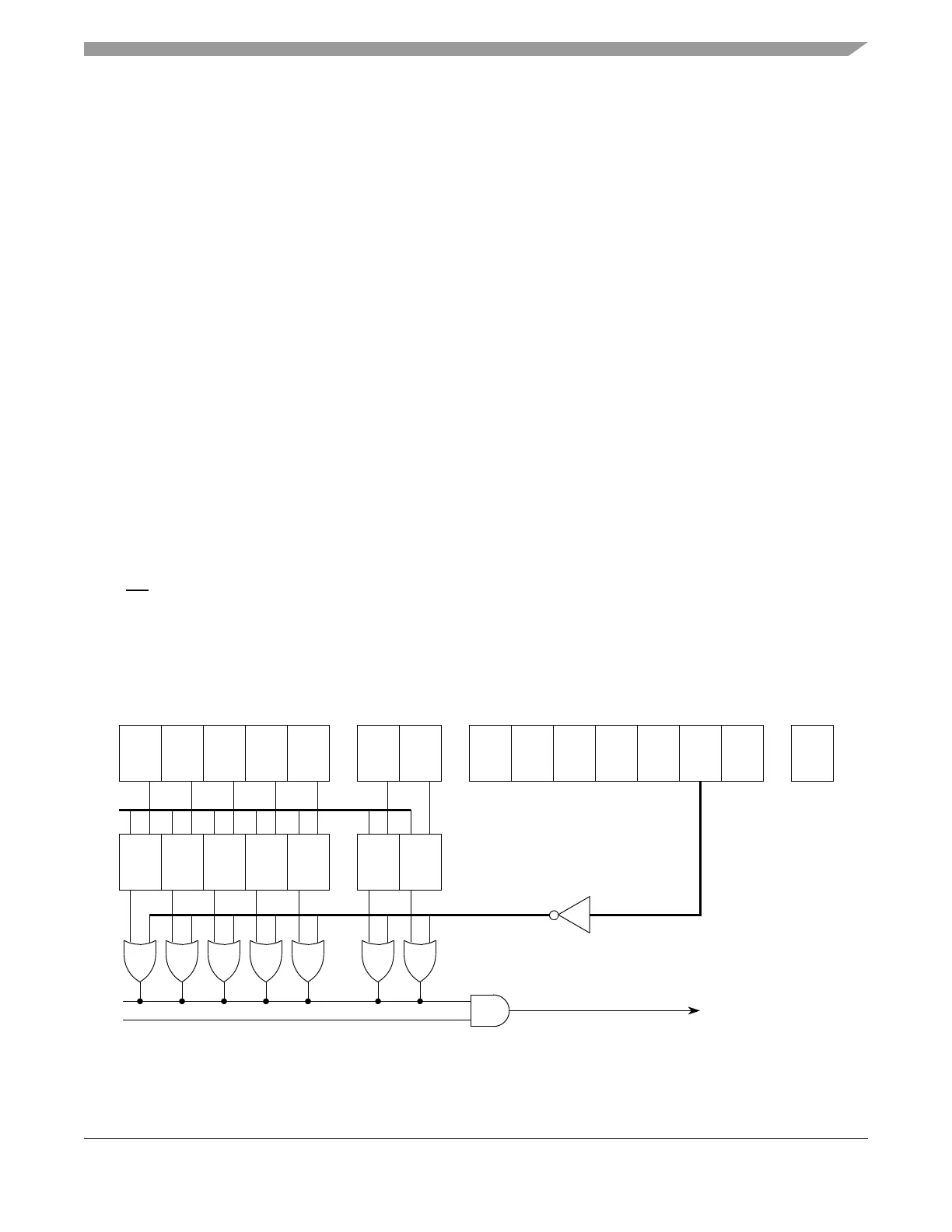
Each CS bank is configured via its own pair of base and option registers. Each time an internal to external
bus cycle access is requested, the internal address is compared with the base address of each valid base
register (with 17 bits having mask). See Figure 12-7. If a match is found, the attributes defined for this
bank in its BR and OR are used to control the memory access. If a match is found in more than one bank,
the lowest bank matched handles the memory access. For example, bank 0 is selected over bank 1.
Figure 12-7. Bank Base Address and Match Structure
BA
[0]
Comp
BA
[1]
Comp
BA
[2]
Comp
BA
[3]
Comp
BA
[4]
Comp
• • •
BA
[15]
Comp
BA
[16]
Comp
AM
[0]
AM
[1]
AM
[2]
AM
[3]
AM
[4]
AM
[5]
• • •
AM
[6]
AM
[16]
• • •
A[0:16]
AM[0:16]
Match
Address MaskBase Address
• • •