MPC5553/MPC5554 Microcontroller Reference Manual, Rev. 5
12-24 Freescale Semiconductor
The write/byte enable lines affected in a transaction for a 32-bit port (PS = 0) and a 16-bit port (PS = 1)
are shown in Table 12-13. Only big-endian byte ordering is supported by the EBI.
12.4.1.14 Two Write/Byte Enable (WE/BE) Signals — 324 BGA of MPC5553 Only
In the 324 BGA of the MPC5553, the functionality of the WE[0:1]/BE[0:1] signals depends on the value
of the WEBS bit in the corresponding base register. Setting WEBS to 1 configures these pins as BE[0:1],
while resetting it to 0 configures them as WE[0:1]. WE[0:1] are asserted only during write accesses, while
BE[0:1] is asserted for both read and write accesses. The timing of the WE[0:1]/BE[0:1] signals remains
the same in either case.
The upper write/byte enable (WE
0/BE0) indicates that the upper eight bits of the data bus (DATA[0:7])
contain valid data during a write/read cycle. The lower write/byte enable (WE1/BE1) indicates that the
lower eight bits of the data bus (DATA[8:15]) contain valid data during a write/read cycle.
The write/byte enable lines affected in a transaction are shown below in Table 12-14. Only big endian byte
ordering is supported by the EBI.
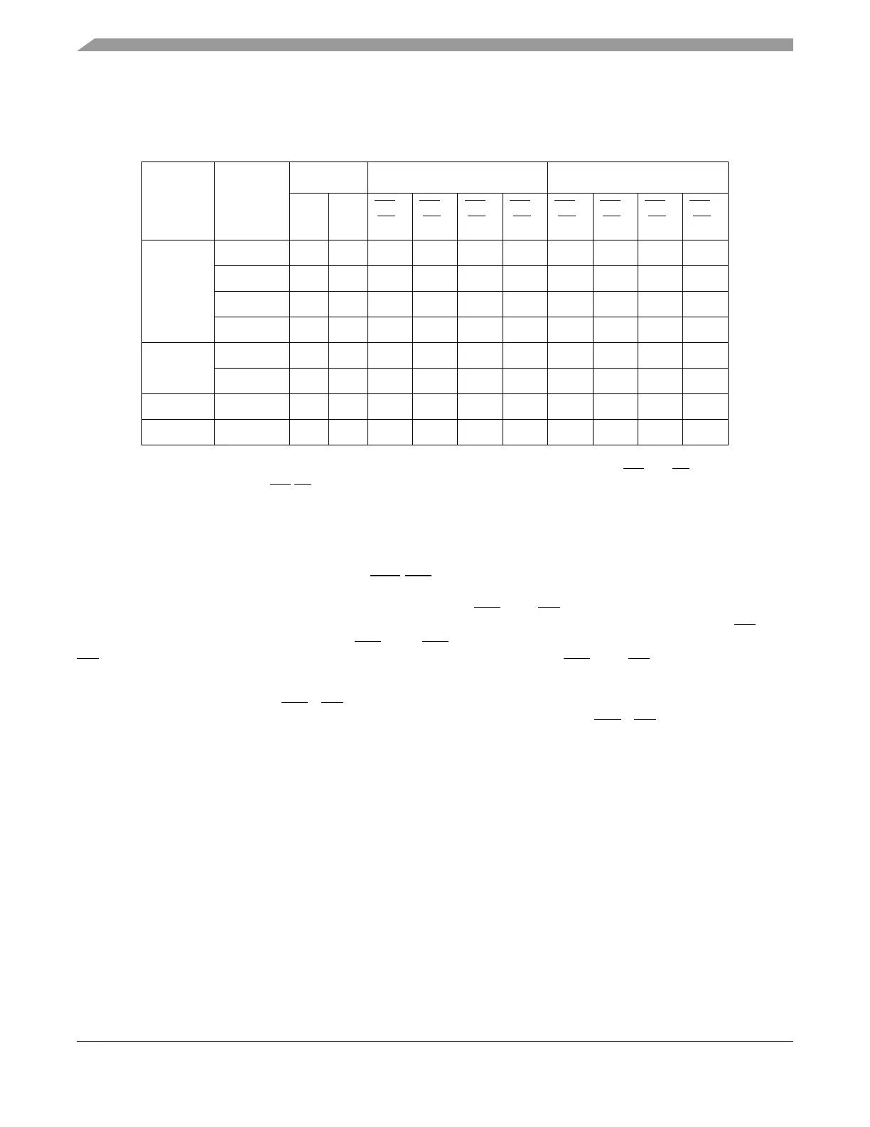
Table 12-13. Write/Byte Enable Signals Function -- 416 BGA
Transfer
Size
TSIZ[0:1]
Address 32-Bit Port Size 16-Bit Port Size
1
1
Also applies when DBM=1 for 16-bit data bus mode.
A30 A31
WE
0/
BE
0
WE
1/
BE
1
WE
2/
BE
2
WE
3/
BE
3
WE
0/
BE
0
WE
1/
BE
1
WE
2/
BE
2
WE
3/
BE
3
Byte 01 00X ———X ———
01 01—X ———X ——
01 10——X —X ———
01 11———X X——
16-bit 10 00XX——XX——
10 10——XXXX——
32-bit 00 00XXXXX
2
2
This case consists of two 16-bit external transactions, but for both transactions the WE[0:1]/BE[0:1]
signals are the only WE/BE signals affected.
NOTE: All areas of the table, both shaded and clear, apply to the 416 BGA package of the MPC5553 and
to the MPC5554.
NOTE: “X” indicates that valid data is transferred on these bits.
X
2
——
Burst 00 00XXXXXX——