MPC5553/MPC5554 Microcontroller Reference Manual, Rev. 5
Freescale Semiconductor 14-29
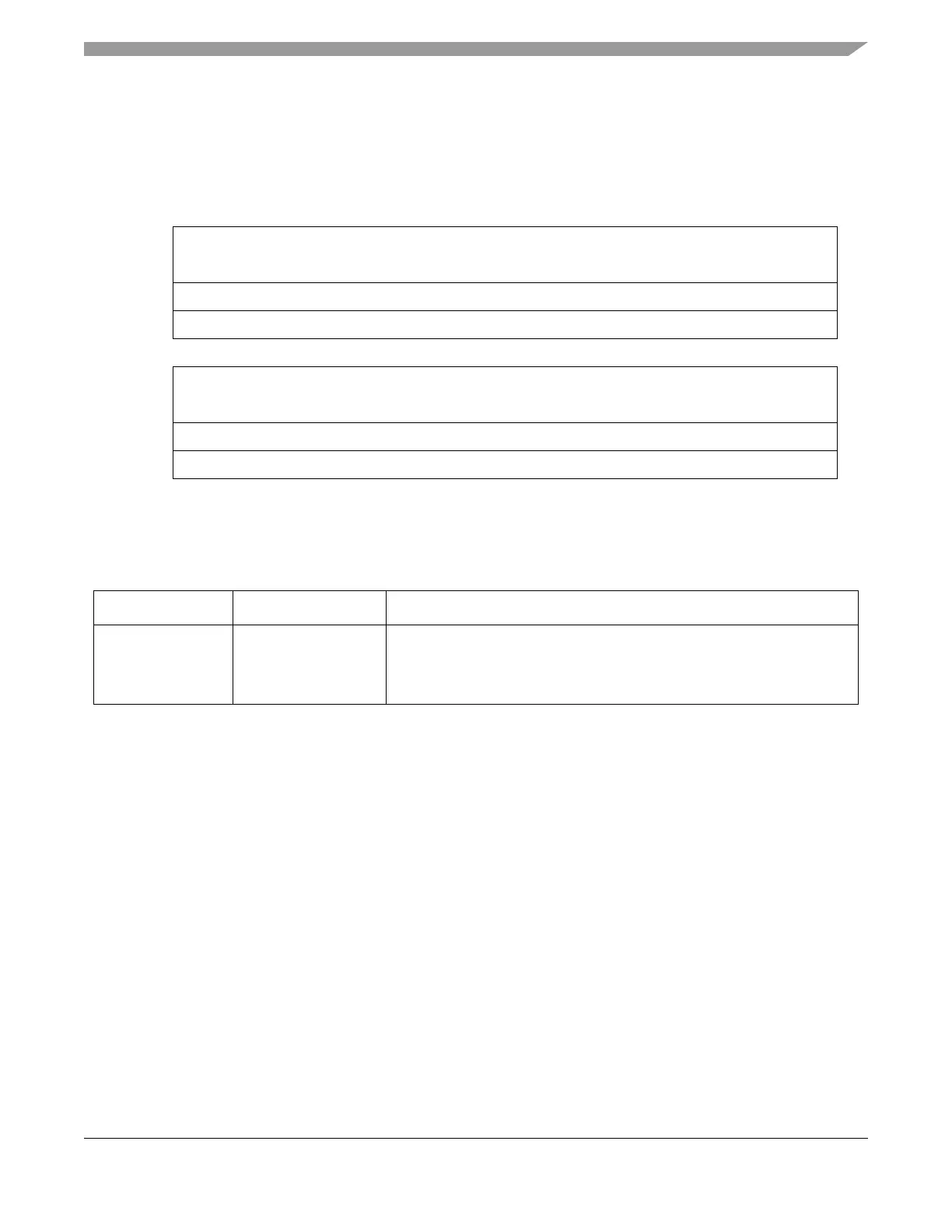
14.3.4.2.17 Descriptor Group Lower Address (GALR)
The GALR register is written by the user. This register contains the lower 32 bits of the 64-bit hash table
used in the address recognition process for receive frames with a multicast address. This register must be
initialized by the user.
14.3.4.2.18 FIFO Transmit FIFO Watermark Register (TFWR)
The TFWR is a 32-bit read/write register with one 2-bit field programmed by the user to control the
amount of data required in the transmit FIFO before transmission of a frame can begin. This allows the
user to minimize transmit latency (TFWR = 0x) or allow for larger bus access latency (TFWR = 11) due
to contention for the system bus. Setting the watermark to a high value will minimize the risk of transmit
FIFO underrun due to contention for the system bus. The byte counts associated with the TFWR field may
need to be modified to match a given system requirement (worst case bus access latency by the transmit
data DMA channel).
0 12 3 4 5 6 7 8 9101112131415
R GADDR2
W
ResetUUUUUUUUUUUUUUU U
Address Base + 0x0124
16 17 18 19 20 21 22 23 24 25 26 27 28 29 30 31
R GADDR2
W
ResetUUUUUUUUUUUUUUU U
Address Base + 0x0124
1
“U” signifies a bit that is uninitialized.
Figure 14-19. Descriptor Group Lower Address Register (GALR)
Table 14-22. GALR Field Descriptions
Bits Name Description
0–31 GADDR2 The GADDR2 register contains the lower 32 bits of the 64-bit hash table
used in the address recognition process for receive frames with a multicast
address. Bit 31 of GADDR2 contains hash index bit 31. Bit 0 of GADDR2
contains hash index bit 0.