MPC5553/MPC5554 Microcontroller Reference Manual, Rev. 5
14-30 Freescale Semiconductor
14.3.4.3 FIFO Receive Bound Register (FRBR)
The FRBR is a 32-bit register with one 8-bit field that the user can read to determine the upper address
bound of the FIFO RAM. Drivers can use this value, along with the FRSR register, to appropriately divide
the available FIFO RAM between the transmit and receive data paths.
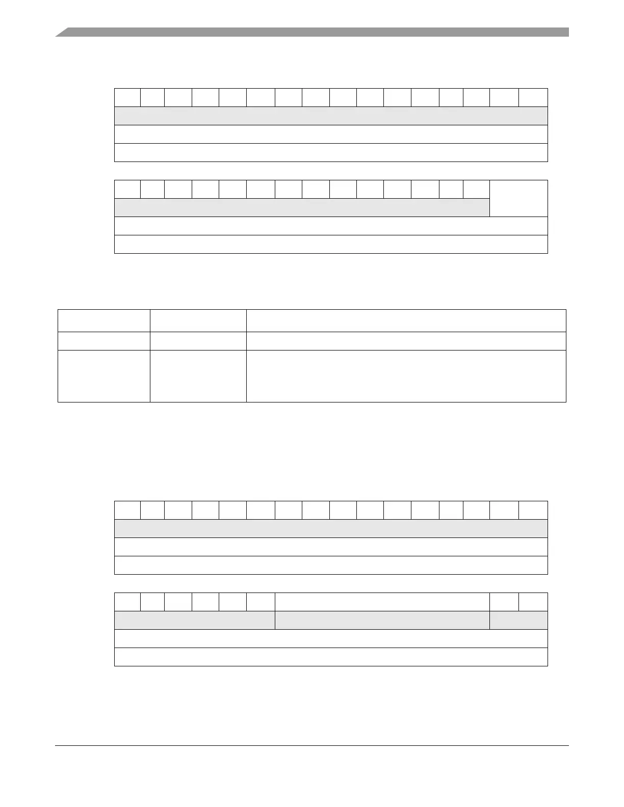
0 1 2 3 4 5 6 7 8 9 10 11 12 13 14 15
R000000000000000 0
W
Reset000000000000000 0
Address Base + 0x0144
16 17 18 19 20 21 22 23 24 25 26 27 28 29 30 31
R00000000000000X_WMRK
W
Reset000000000000000 0
Address Base + 0x0144
Figure 14-20. FIFO Transmit FIFO Watermark Register (TFWR)
Table 14-23. TFWR Field Descriptions
Bits Name Descriptions
0–29 — Reserved, should be cleared.
30–31 X_WMRK Number of bytes written to transmit FIFO before transmission of a frame begins
0x 64 bytes written
10 128 bytes written
11 192 bytes written
0 1 2 3 4 5 6 7 8 9 10 11 12 13 14 15
R000000000000000 0
W
Reset000000000000000 0
Address Base + 0x014C
16 17 18 19 20 21 22 23 24 25 26 27 28 29 30 31
R 0 0 0 0 0 0 R_BOUND 0 0
W
Reset000001100000000 0
Address Base + 0x014C
Figure 14-21. FIFO Receive Bound Register (FRBR)