MPC5553/MPC5554 Microcontroller Reference Manual, Rev. 5
17-52 Freescale Semiconductor
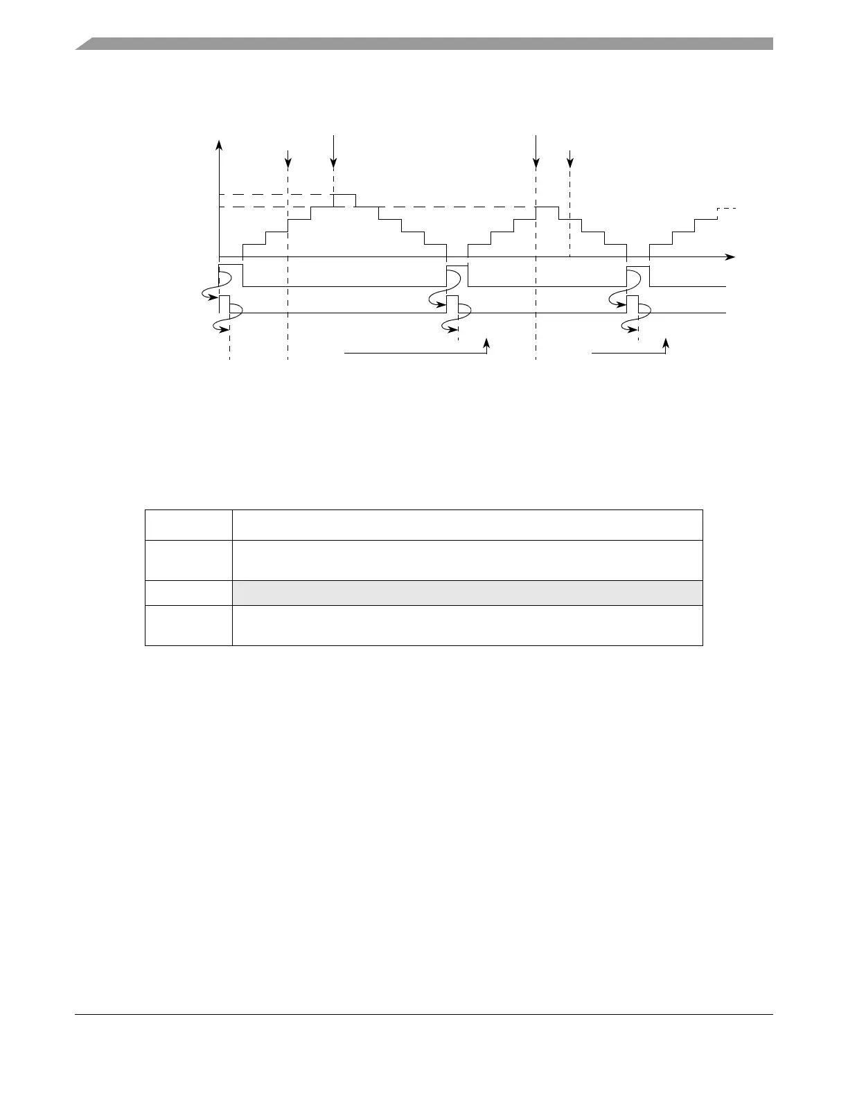
Figure 17-40. eMIOS MCB Mode Example — Up/Down Operation A1 Register Update
17.4.4.4.16 Output Pulse Width and Frequency Modulation, Buffered Mode (OPWFMB)
(MPC5553 Only)
This mode generates waveforms with variable duty cycle and frequency. The internal channel counter is
automatically selected as the time base, A1 sets the duty cycle and B1 determines the frequency. Both A1
and B1 are double buffered to allow smooth signal generation when changing the register values
asynchronously. Both 0% and 100% duty cycles are supported.
In order to provide smooth and consistent channel operation, this mode differs substantially from the
OPWFM mode. The main differences are in how A1 and B1 are updated, the delay from the A1 match to
the output flip-flop transition, and the range of the internal counter which ranges from 1 up to B1 value.
When a match on comparator A occurs, the output register is set to the value of EDPOL. When a match
on comparator B occurs, the output register is set to the complement of EDPOL. A B1 match also causes
the internal counter to transition to 1, thus re-starting the counter cycle.
Figure 17-41 shows an example of OPWFMB mode operation. Note that the output flip-flop transition
occurs when the A1 or B1 match signal is negated, as detected by the negative edge of the A1 and B1 match
signals. For example, if register A1 is set to 0x000004, the output flip-flop transitions 4 counter periods
after the cycle starts, plus one system clock cycle. Note that in the example shown in Figure 17-41 the
prescaler ratio is set to two (refer to Section 17.5.3, “Time Base Generation).
Table 17-29. Mode of Operation: OPWFMB Mode
MODE[0:6] Unified Channel Mode of Operation
0b1011000 Output pulse width and frequency modulation, buffered
(FLAG set at match of internal counter and comparator B)
0b1011001
Reserved
0b1011010 Output pulse width and frequency modulation, buffered
(FLAG set at match of internal counter and comparator A or comparator B)
EMIOS_CCNTR
Time
Write to A2
Match A1
Match A1
Write to A2
0x000001
0x000005
0x000006
0x000005
A2 Value
A1 Value
0x000006
0x000005
Selected Counter = 1
A1 Load Signal
0x000006 0x000006
0x000006
Cycle n Cycle n+1 Cycle n+2
A2value transferred to A1 according to OUn bit (the transfer is triggered by the A1 load signal)