MPC5553/MPC5554 Microcontroller Reference Manual, Rev. 5
Freescale Semiconductor 17-51
Flags are generated only at an A1 match if MODE[5] is 0. If MODE[5] is 1, flags are also generated at the
cycle boundary.
Figure 17-38. eMIOS MCB Mode Example — Up/Down Operation
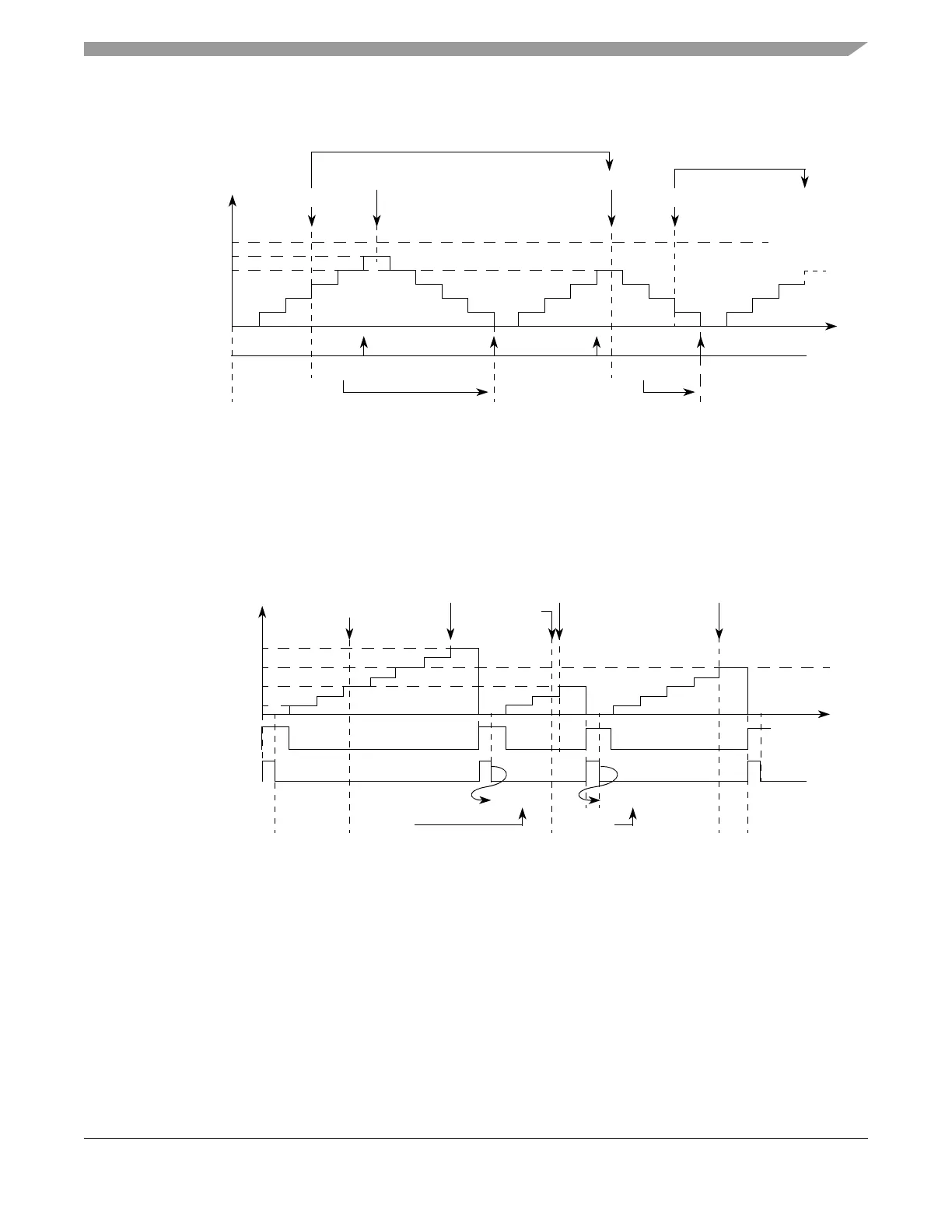
Figure 17-39 provides a more detailed illustration of the A1 update process in up counter mode. The A1
load signal is generated based on the detection of the internal counter reaching one, and has the duration
of one system clock cycle. Note that during the load pulse A1 still holds its previous value. It is actually
updated at the second system clock cycle.
Figure 17-39. eMIOS MCB Mode Example — Up Operation A1 Register Update
Figure 17-40 illustrates the A1 register update process in up/down counter mode. Note that A2 can be
written at any time within cycle (n) in order to be used in cycle (n+1). Thus A1 receives the new value at
the next cycle boundary. The EMIOS_OUDR[n] bits can be used to disable the update of A1 register.
Time
Write to A2
Match A1
Match A1
Write to A2
0x000001
0x000005
0x000006
0x000007
FLAG Set Event
0x000005 0x000007
A2 Value
A1 Value
0x000006
0x000005
0x000007
EMIOS_CCNTRn
A2value transferred to A1 according to OUn bit.
A1 Value 0x000008
0x000008
0x000001
EMIOS_CCNTR
0x000004
0x000006
A2 Value 0x000008 0x000004 0x000006
0x000002
0x000004 0x000006
Write to A2
A1 Load Signal
1
8
4
6
Selected Counter = 1
Time
Cycle n
Cycle n+1
Cycle n+2
Match A1 Match A1Match A1
Write to A2
A2value transferred to A1 according to OUn bit.