MPC5553/MPC5554 Microcontroller Reference Manual, Rev. 5
Freescale Semiconductor 17-63
Figure 17-51. eMIOS OPWMB Mode Example — 0% Duty Cycle
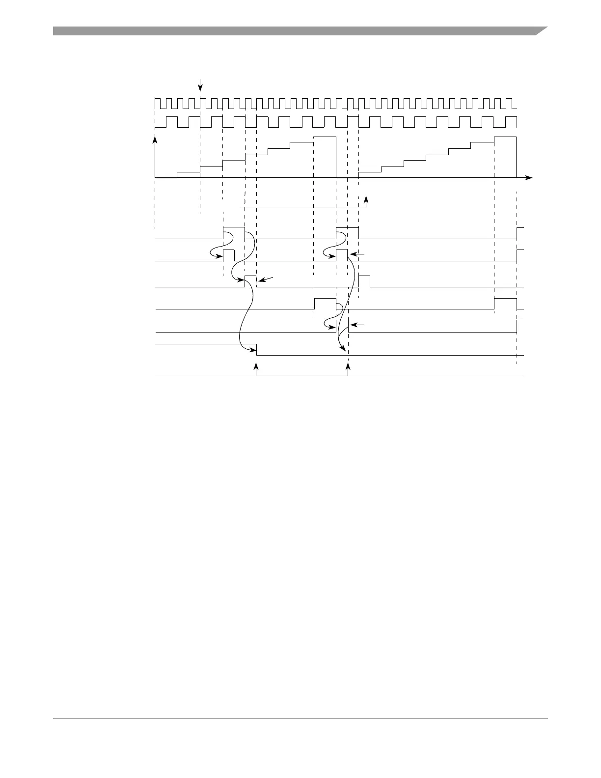
Figure 17-52 shows the operation of the OPWMB mode with the output disable signal asserted. The output
disable forces a transition in the output flip-flop to the EDPOL bit value. After the output disable is
negated, the output flip-flop is allowed to transition at the next A1 or B1 match. The output disable does
not modify the flag bit behavior. Note that there is one system clock delay between the assertion of the
output disable signal and the transition of the output flip-flop.
1
4
A1 Match Nega-
A1 Value 0x000004
A1 Match
Output Flip-Flop
Selected
Time
B1 Match
B1 Match
B1 Value 0x000006
System Clock
Prescaled Clock
A2 Value 0x000000
0x000000
A1 Match Positive Edge Detect
1
8
FLAG Bit Set
EDPOL = 0
A1 Match Negative
B1 Match Negative
A1 Match Positive
Edge Detection
Edge Detection
Edge Detection
Negative Edge Detect
Cycle n Cycle n+1
Write to A2
8
tive Edge Detect
Counter Bus