MPC5553/MPC5554 Microcontroller Reference Manual, Rev. 5
Freescale Semiconductor 19-49
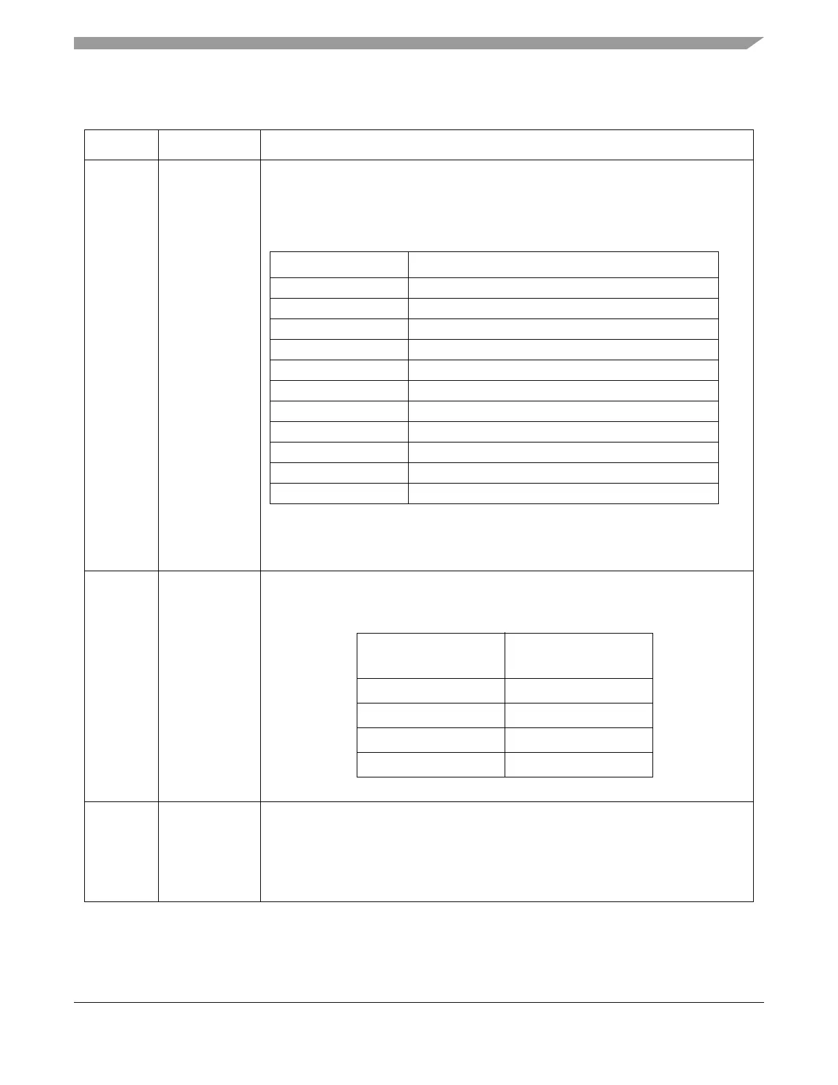
8–11 MESSAGE_TAG
[0:3]
MESSAGE_TAG field. Allows the eQADC to separate returning results into different
RFIFOs. When the eQADC transfers a command, the MESSAGE_TAG is included as part
of the command. Eventually the external device/on-chip ADC returns the result with the
same MESSAGE_TAG. The eQADC separates incoming messages into different RFIFOs
by decoding the MESSAGE_TAG of the incoming data.
12–13 LST
[0:1]
Long sampling time. These two bits determine the duration of the sampling time in ADC
clock cycles.
Note: For external mux mode, 64 or 128 sampling cycles is recommended.
14 TSR Time stamp request. TSR indicates the request for a time stamp. When TSR is asserted,
the on-chip ADC control logic returns a time stamp for the current conversion command
after the conversion result is sent to the RFIFOs. See Section 19.4.5.3, “Time Stamp
Feature,” for details.
0 Return conversion result only.
1 Return conversion time stamp after the conversion result.
Table 19-34. On-Chip ADC Field Descriptions:
Conversion Command Message Format (Continued)
Bits Name Description
MESSAGE_TAG[0:3] MESSAGE_TAG Meaning
0b0000 Result is sent to RFIFO 0
0b0001 Result is sent to RFIFO 1
0b0010 Result is sent to RFIFO 2
0b0011 Result is sent to RFIFO 3
0b0100 Result is sent to RFIFO 4
0b0101 Result is sent to RFIFO 5
0b0110–0b0111 Reserved
0b1000 Null message received
0b1001 Reserved for customer use.
1
1
These messages are treated as null messages. Therefore, they must obey the
format for incoming null messages and return valid BUSY0/1 fields. Refer to
Section , “ Null Message Format for External Device Operation.”
0b1010 Reserved for customer use.
1
0b1011–0b1111 Reserved
LST[0:1]
Sampling cycles
(ADC Clock Cycles)
0b00 2
0b01 8
0b10 64
0b11 128