MPC5553/MPC5554 Microcontroller Reference Manual, Rev. 5
Freescale Semiconductor 20-47
The source for the SIN input of a DSPI can be a pin or the SOUT of any of the other three (for the
MPC5554) DSPIS or two (for the MPC5553) DSPIs. The source for the SS input of a DSPI can be a pin
or the PCS0 signal from any of the other DSPIs. The source for the SCK input of a DSPI can be a pin or
the SCK output of any of the other DSPIs. The source for the hardware trigger (ht) input can be the MTRIG
signal from any of the other DSPIs. The DSPI input select register (SIU_DSR) selects the source for each
DSPI SIN, SS, SCK, and ht signal individually.
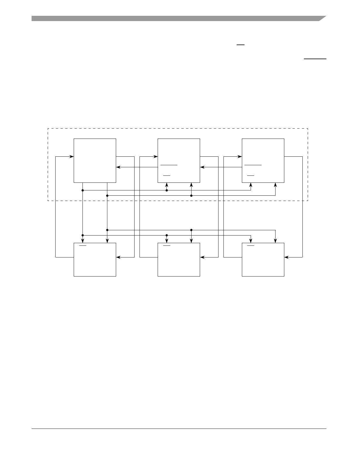
20.4.4.7.2 Parallel Chaining
Parallel chaining allows the PCS and SCK signals from a master DSPI to be shared by internal slave DSPIs
and external slave SPI devices. Signal sharing reduces DSPI pin utilization. An example of a parallel chain
is shown in Figure 20-27 (for the MPC5554) or Figure 20-28 (for the MPC5553).
Figure 20-27. Example of Parallel Chaining of DSPIs in the MPC5554
SOUT
ht
SCK
SIN
MTRIG
SS
MPC5554
DSPI_A
SOUT
ht
SCK
SIN
PCS0
SIN_A
PCS_A0
SCK_A
SOUT_A
SIN_B
(Master)
DSPI_B
(Slave)
SOUT
SCK
SIN
MTRIG
SS
DSPI_C
(Slave)
SOUT_B
SIN_C
SOUT_C
SCKSS
SIN
Slave Device
SPI
SOUT
SCKSS
SIN
Slave Device
SPI
SOUT
SCKSS
SIN
Slave Device
SPI
SOUT