MPC5553/MPC5554 Microcontroller Reference Manual, Rev. 5
21-28 Freescale Semiconductor
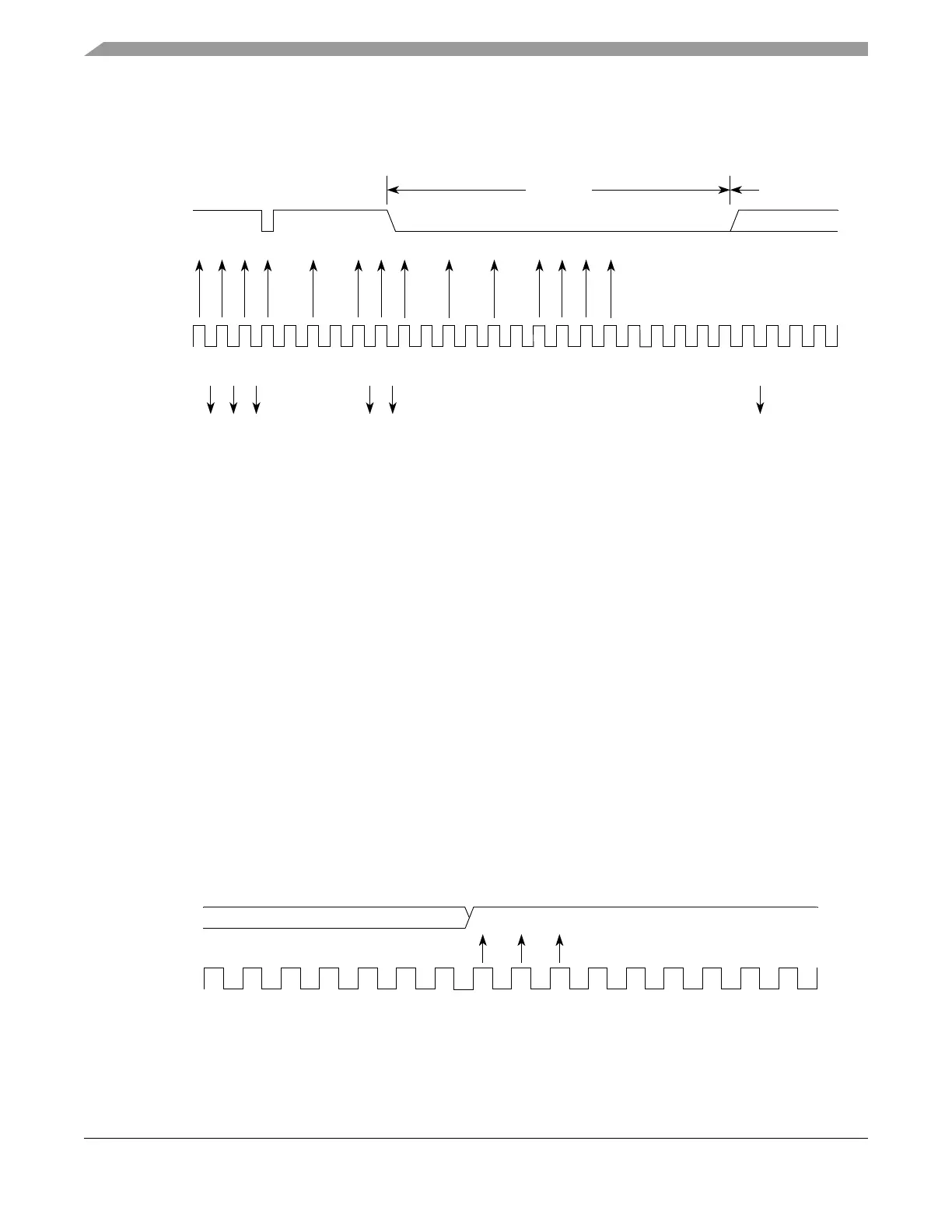
In Figure 21-18 the verification samples RT3 and RT5 determine that the first low detected was noise and
not the beginning of a start bit. The RT clock is reset and the start bit search begins again. The noise flag
is not set because the noise occurred before the start bit was found.
Figure 21-18. Start Bit Search Example
21.4.5.4 Framing Errors
If the data recovery logic sets the framing error flag, ESCIx_SR[FE], it does not detect a logic 1 where the
stop bit should be in an incoming frame. A break character also sets the FE flag because a break character
has no stop bit. The FE flag is set at the same time that the RDRF flag is set.
21.4.5.5 Baud Rate Tolerance
A transmitting device may be operating at a baud rate below or above the receiver baud rate. Accumulated
bit time misalignment can cause one of the three stop bit data samples (RT8, RT9, and RT10) to fall outside
the actual stop bit. A noise error will occur if the RT8, RT9, and RT10 samples are not all the same logical
values. A framing error will occur if the receiver clock is misaligned in such a way that the majority of the
RT8, RT9, and RT10 stop bit samples are a logic zero.
As the receiver samples an incoming frame and re-synchronizes the RT clock on any valid falling edge
within the frame. Re-synchronization within frames will correct a misalignment between transmitter bit
times and receiver bit times.
21.4.5.5.1 Slow Data Tolerance
Figure 21-19 shows how much a slow received frame can be misaligned without causing a noise error or
a framing error. The slow stop bit begins at RT8 instead of RT1 but arrives in time for the stop bit data
samples at RT8, RT9, and RT10.
Figure 21-19. Slow Data
RT Clock
1110 1 11 000
RT1
RT1
RT1 RT2
RT1
RT4
RT3 RT5
RT1 RT2 RT4 RT6 RT8 RT10 RT12 RT14 RT16 RT2
RT1 RT3 RT5 RT7 RT9 RT11 RT13 RT15 RT1 RT3
Reset
RT Clock
RT Clock
Count
RXD Input
Signal
Samples
Start Bit LSB
0
0 0 0
RT1
Receiver
RT Clock
RT2 RT3 RT4 RT5 RT6 RT7 RT8 RT9 RT10 RT11 RT12 RT13 RT14 RT15 RT16
MSB STOP
Data Samples