RM0091 Reset and clock control (RCC)
Doc ID 018940 Rev 1 113/742
7.4.12 Clock configuration register 2 (RCC_CFGR2)
Address: 0x2C
Reset value: 0x0000 0000
Access: no wait states, word, half-word and byte access
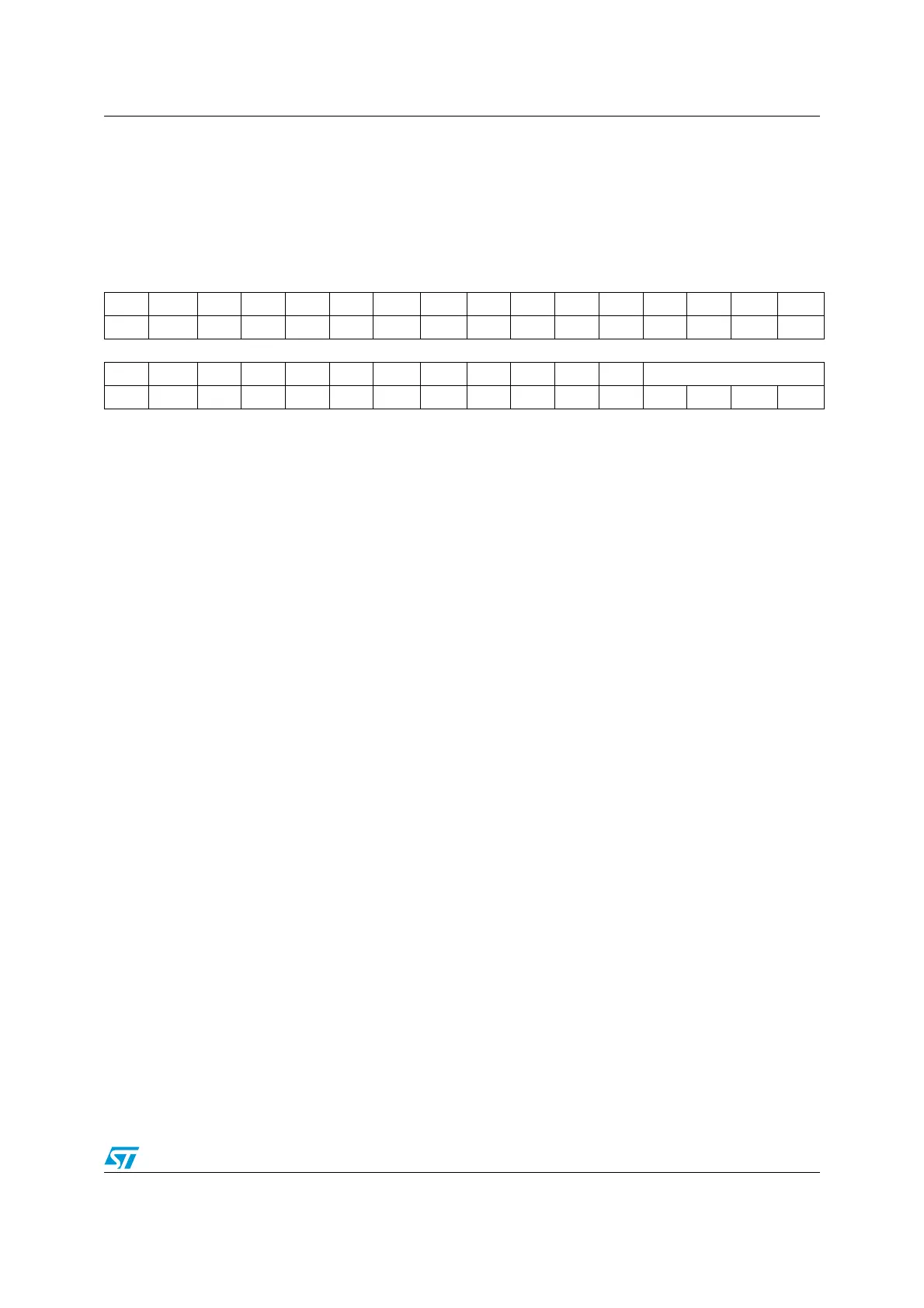
31 30 29 28 27 26 25 24 23 22 21 20 19 18 17 16
Res Res Res Res Res Res Res Res Res Res Res Res Res Res Res Res
15 14 13 12 11 10 9 8 7 6 5 4 3 2 1 0
Res Res Res Res Res Res Res Res Res Res Res Res PREDIV[3:0]
rw rw rw rw
Bits 31:4 Reserved, must be kept at reset value.
Bits 3:0 PREDIV[3:0] PREDIV division factor
These bits are set and cleared by software to select PREDIV1 division factor. They can be
written only when the PLL is disabled.
Note: Bit 0 is the same bit as bit17 in Clock configuration register (RCC_CFGR), so modifying
bit17 Clock configuration register (RCC_CFGR) aslo modifies bit 0 in Clock
configuration register 2 (RCC_CFGR2) ( for compatibility with other STM32 products)
0000: HSE input to PLL not divided
0001: HSE input to PLL divided by 2
0010: HSE input to PLL divided by 3
0011: HSE input to PLL divided by 4
0100: HSE input to PLL divided by 5
0101: HSE input to PLL divided by 6
0110: HSE input to PLL divided by 7
0111: HSE input to PLL divided by 8
1000: HSE input to PLL divided by 9
1001: HSE input to PLL divided by 10
1010: HSE input to PLL divided by 11
1011: HSE input to PLL divided by 12
1100: HSE input to PLL divided by 13
1101: HSE input to PLL divided by 14
1110: HSE input to PLL divided by 15
1111: HSE input to PLL divided by 16