RM0091 Embedded Flash memory
Doc ID 018940 Rev 1 43/742
3.2.2 Read operations
The embedded Flash module can be addressed directly, as a common memory space. Any
data read operation accesses the content of the Flash module through dedicated read
senses and provides the requested data.
The instruction fetch and the data access are both done through the same AHB bus. Read
accesses can be performed with the following options managed through the Flash access
control register (FLASH_ACR):
● Instruction fetch: Prefetch buffer enabled for a faster CPU execution.
● Latency: number of wait states for a correct read operation (from 0 to 1)
Instruction fetch
The Cortex-M0 fetches the instruction over the AHB bus. The prefetch block aims at
increasing the efficiency of instruction fetching.
Prefetch buffer
The prefetch buffer is 3 blocks wide where each block consists of 8 bytes. The prefetch
blocks are direct-mapped. A block can be completely replaced on a single read to the Flash
memory as the size of the block matches the bandwidth of the Flash memory.
The implementation of this prefetch buffer makes a faster CPU execution possible as the
CPU fetches one word at a time with the next word readily available in the prefetch buffer.
This implies that the acceleration ratio will be of the order of 2 assuming that the code is
aligned at a 64-bit boundary for the jumps.
Prefetch controller
The prefetch controller decides to access the Flash memory depending on the available
space in the prefetch buffer. The Controller initiates a read request when there is at least
one block free in the prefetch buffer.
After reset, the state of the prefetch buffer is on.
The prefetch buffer should be switched on/off only when SYSCLK is lower than 24 MHz and
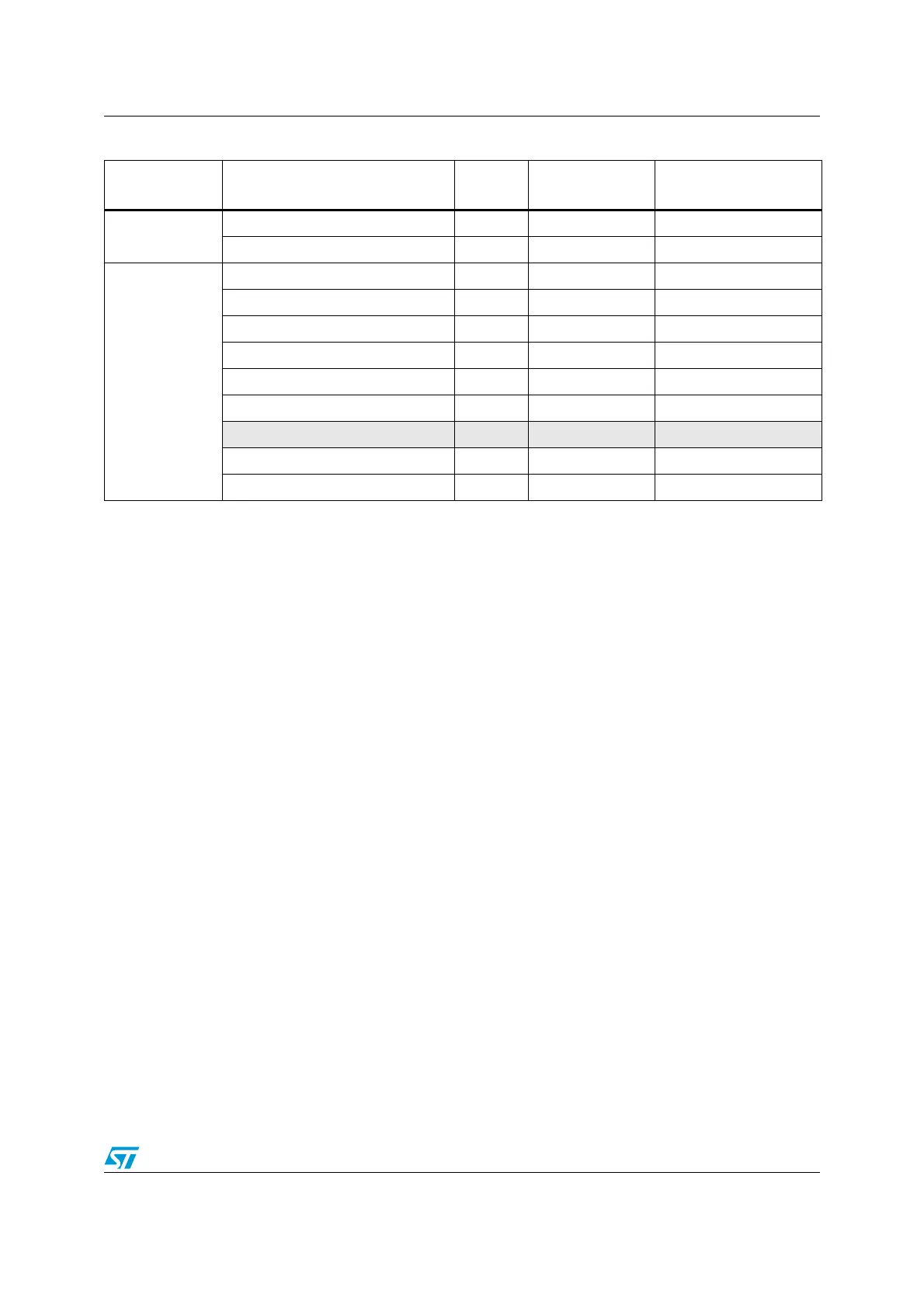
Information block
0x1FFF EC00- 0x1FFF F7FF 3 Kbytes System memory
0x1FFF F800 - 0x1FFF F80B 6 Option bytes
Flash memory
interface
registers
0x4002 2000 - 0x4002 2003 4 FLASH_ACR
0x4002 2004 - 0x4002 2007 4 FLASH_KEYR
0x4002 2008 - 0x4002 200B 4 FLASH_OPTKEYR
0x4002 200C - 0x4002 200F 4 FLASH_SR
0x4002 2010 - 0x4002 2013 4 FLASH_CR
0x4002 2014 - 0x4002 2017 4 FLASH_AR
0x4002 2018 - 0x4002 201B 4 Reserved
0x4002 201C - 0x4002 201F 4 FLASH_OBR
0x4002 2020 - 0x4002 2023 4 FLASH_WRPR
Table 4. Flash module organization (continued)
Flash area Flash memory addresses
Size
(bytes)
Name Description