RM0091 General-purpose timer (TIM14)
Doc ID 018940 Rev 1 359/742
17.3.3 Clock source
The counter clock is provided by the Internal clock (CK_INT) source.
The CEN (in the TIMx_CR1 register) and UG bits (in the TIMx_EGR register) are actual
control bits and can be changed only by software (except for UG that remains cleared
automatically). As soon as the CEN bit is written to 1, the prescaler is clocked by the internal
clock CK_INT.
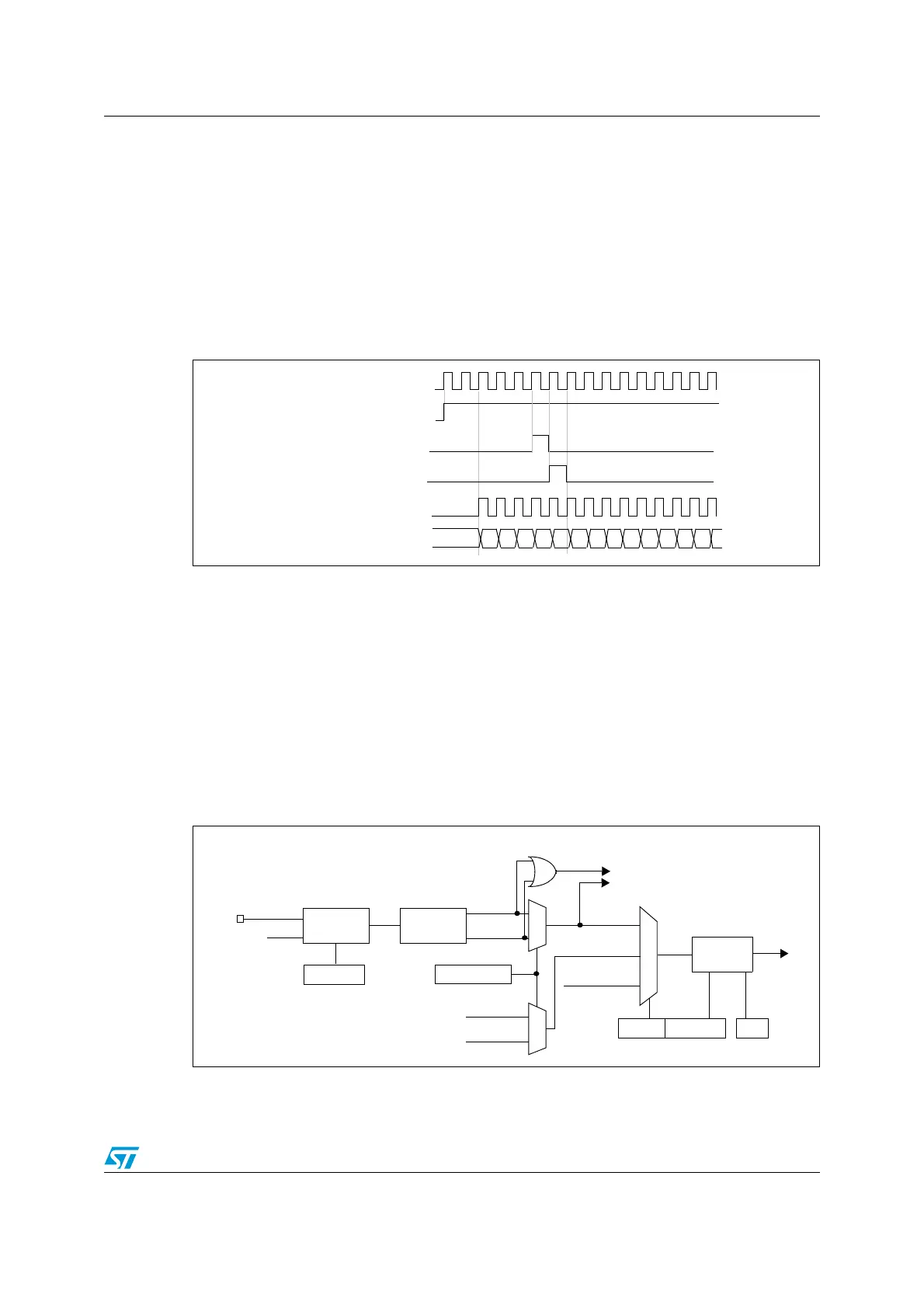
Figure 146 shows the behavior of the control circuit and the upcounter in normal mode,
without prescaler.
Figure 146. Control circuit in normal mode, internal clock divided by 1
17.3.4 Capture/compare channels
Each Capture/Compare channel is built around a capture/compare register (including a
shadow register), a input stage for capture (with digital filter, multiplexing and prescaler) and
an output stage (with comparator and output control).
Figure 147 to Figure 149 give an overview of one capture/compare channel.
The input stage samples the corresponding TIx input to generate a filtered signal TIxF.
Then, an edge detector with polarity selection generates a signal (TIxFPx) which can be
used as trigger input by the slave mode controller or as the capture command. It is
prescaled before the capture register (ICxPS).
Figure 147. Capture/compare channel (example: channel 1 input stage)
The output stage generates an intermediate waveform which is then used for reference:
OCxRef (active high). The polarity acts at the end of the chain.
CK_INT
00
Counter clock = CK_CNT = CK_PSC
Counter register
01 02 03 04 05 06 0732 33 34 35 3631
CEN=CNT_EN
UG
CNT_INIT
TI1
0
1
TIMx_CCER
CC1P/CC1NP
divider
/1, /2, /4, /8
ICPS[1:0]
TI1F_ED
filter
ICF[3:0]
downcounter
TIMx_CCMR1
Edge
Detector
TI1F_Rising
TI1F_Falling
to the slave mode controller
TI1FP1
11
01
TIMx_CCMR1
CC1S[1:0]
IC1
TI2FP1
TRC
(from channel 2)
(from slave mode
controller)
10
f
DTS
TIMx_CCER
CC1E
IC1PS
TI1F
0
1
TI2F_rising
TI2F_falling
(from channel 2)