Inter-integrated circuit (I
2
C) interface RM0091
474/742 Doc ID 018940 Rev 1
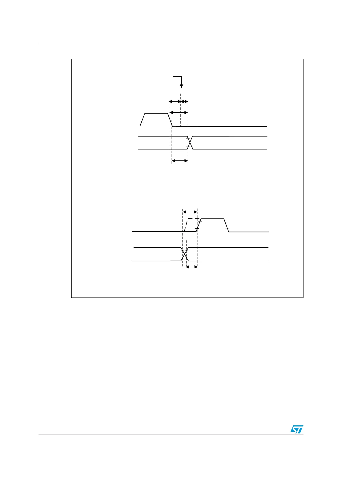
Figure 198. Setup and hold timings
● When the SCL falling edge is internally detected, a delay is inserted before sending
SDA output. This delay is
t
SDADEL
= SDADEL x t
PRESC
where t
PRESC
= (PRESC+1) x t
I2CCLK.
T
SDADEL
impacts the hold time t
HD;DAT .
The total SDA output delay is:
t
SYNC1
+ [ SDADEL x (PRESC+1) x t
I2CCLK
]
t
SYNC1
duration depends on these parameters:
– SCL falling slope
– When enabled, input delay brought by the analog filter: t
AF
.
50ns < t
AF
< 260 ns.
– When enabled, input delay brought by the digital filter: t
DNF
= DNF x t
I2CCLK
– Delay due to SCL synchronization to I2CCLK clock (2 to 3 I2CCLK periods)
In order to bridge the undefined region of the SCL falling edge, you must program SDADEL
in such a way that:
{t
f (max)
+t
HD;DAT (min)
-50ns - [(DNF +2 ) x t
I2CCLK
]} / {(PRESC +1) x t
I2CCLK
} <= SDADEL
MS19846V1
t
SYNC1
SCL falling edge internal detection
SDADEL
SDA output delay
SCL
SDA
DATA HOLD TIME
t
h(SDA)
Data hold time
SCLDEL
SCL stretched low by the slave transmitter
SCL
SDA
DATA SETUP TIME
tsu
(SDA)
Data setup time