Serial peripheral interface / inter-IC sound (SPI/I2S) RM0091
642/742 Doc ID 018940 Rev 1
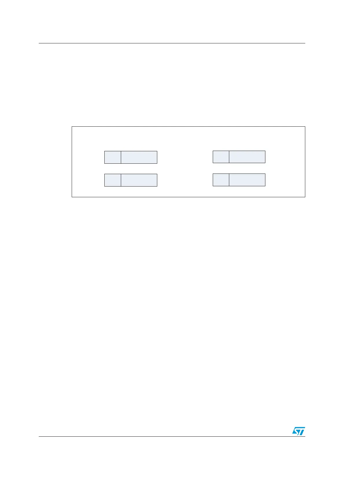
Data frame format
The SPI shift register can be set up to shift out MSB-first or LSB-first, depending on the
value of the LSBFIRST bit. The data frame size is chosen by using the DS bits. It can be set
from 4-bit up to 16-bit length and the setting applies for both transmission and reception.
Whatever the selected data frame size, read access to the FIFO must be aligned with the
FRXTH level. When the SPIx_DR register is accessed, data frames are always right-aligned
into either a byte (if the data fits into a byte) or a word (see Figure 260). During
communication, only bits within the data frame are clocked and transferred.
Figure 260. Data alignment when data length is not equal to 8-bit or 16-bit
Note: The minimum data length is 4 bits. If a data length of less than 4-bits is selected, it is forced
to an 8-bit data frame size.
26.3.6 Initialize SPI
The initialization procedure is almost identical for master and slave. When setting the bit
configuration registers SPIx_CR1 and SPIx_CR2:
1. Select the serial clock baud rate using the BR[2:0] bits (see Note Note:)
2. Set the CPOL and CPHA bits combination to define one of the four relationships
between the data transfer and the serial clock (see Figure 259 and Note )
3. Select a transmission mode by configuring RXONLY, BIDIOE and BIDIMODE (see
Note ).
4. Set the DS bit in order to select the data length for the transfer.
5. Configure the LSBFIRST bit to define the frame format (see Note ).
6. Set SSM, SSI and SSOE according to application needs. In master mode, the internal
NSS signal must stay at a high level during the complete sequence (see
Section 26.3.4: Slave select (NSS) pin management on page 639). In slave mode, the
internal NSS signal must stay at a low level during the complete sequence (see Note ).
7. Set the FRF bit if the TI protocol is required (see Section 26.4.2: TI mode on page 649).
8. Set the NSSP bit if the NSS pulse mode between two data units is required. The CHPA
bit must be set to 1 for this configuration (see Note ).
9. Set the FRXTH bit. The RXFIFO threshold must be aligned to the read access size for
the SPIx_DR register.
10. Initialize LDMA_TX and LDMA_RX bits if DMA is used.
11. Set the CRC polynomial to “in” and set the CRCEN bit if CRC is needed.
12. Set the MSTR bit while the NSS internal signal is at a high level (see Note Note: and
Section 26.3.4: Slave select (NSS) pin management)
13. Enable the SPI by setting the SPE bit (see Note ).
MS19589V1
XXX
000
Data frame
Data frame
XX
00
Data frame
Data frame
TX
RX
TX
RX
7
7
54
54
0
0
15
13 0
14
15
13 0
14
DS <= 8 bits: data is right-aligned on byte
Example: DS = 5 bit
DS > 8 bits: data is right-aligned on 16 bit
Example: DS = 14 bit