RM0091 Embedded Flash memory
Doc ID 018940 Rev 1 57/742
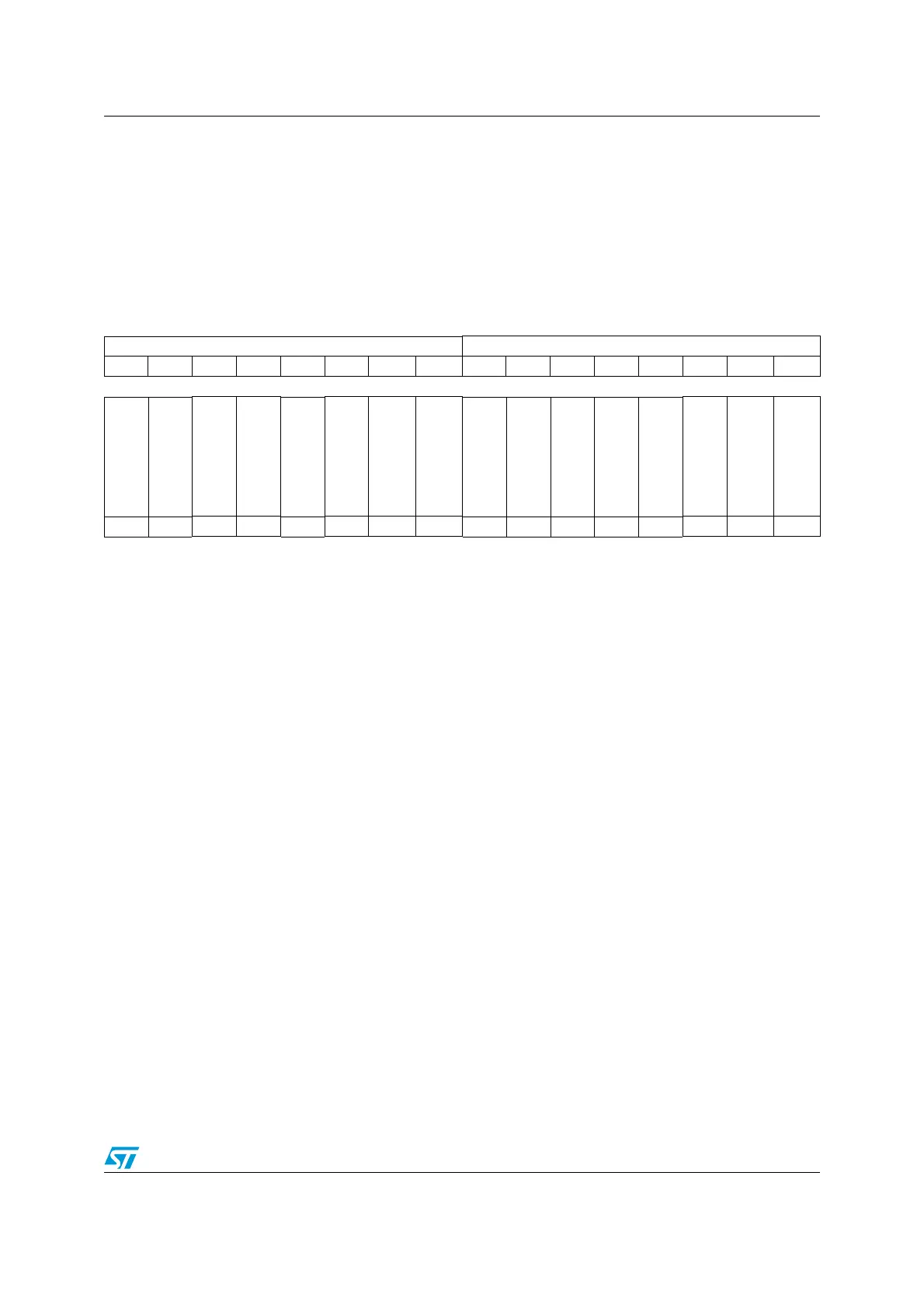
3.5.7 Option byte register (FLASH_OBR)
Address offset 0x1C
Reset value: 0x03FF FFF2
The reset value of this register depends on the value programmed in the option byte and the
OPTERR bit reset value depends on the comparison of the option byte and its complement
during the option byte loading phase.
31 30 29 28 27 26 25 24 23 22 21 20 19 18 17 16
Data1 Data0
rrrrrrr rrrrrrrr r
15 14 13 12 11 10 9 8 7 6 5 4 3 2 1 0
Res.
RAM_PARITY_CHECK
VDDA_MONITOR
nBOOT1
Res.
nRST_STDBY
nRST_STOP
WDG_SW
Res.
Res.
Res.
Res.
Res.
RDPRT2
RDPRT1
OPTERR
rr rr r rr r
Bits 31:24 Data1
Bits 23:16 Data0
Bits 15:8 User option bytes :
Bit 15 : reserved
Bit 14 : RAM_PARITY_CHECK
Bit 13 : VDDA_MONITOR
Bit 12 : nBOOT1
Bit 11 : reserved
Bit 10 : nRST_STDBY
Bit 9 : nRST_STOP
Bit 8 : WDG_SW
Bits 7:3 Reserved, must be kept at reset value.
Bits 2:1 RDPRT[2:1]: Read protection level status
00: Read protection level 0 is enabled (ST production configuration)
01: Read protection level 1 is enabled
11: Read protection level 2 is enabled.
Bit 0 OPTERR: Option byte error
When set, this indicates that the loaded option byte and its complement do not
match. The corresponding byte and its complement are read as 0xFF in the
FLASH_OBR or FLASH_WRPR register.