General-purpose I/Os (GPIO) RM0091
126/742 Doc ID 018940 Rev 1
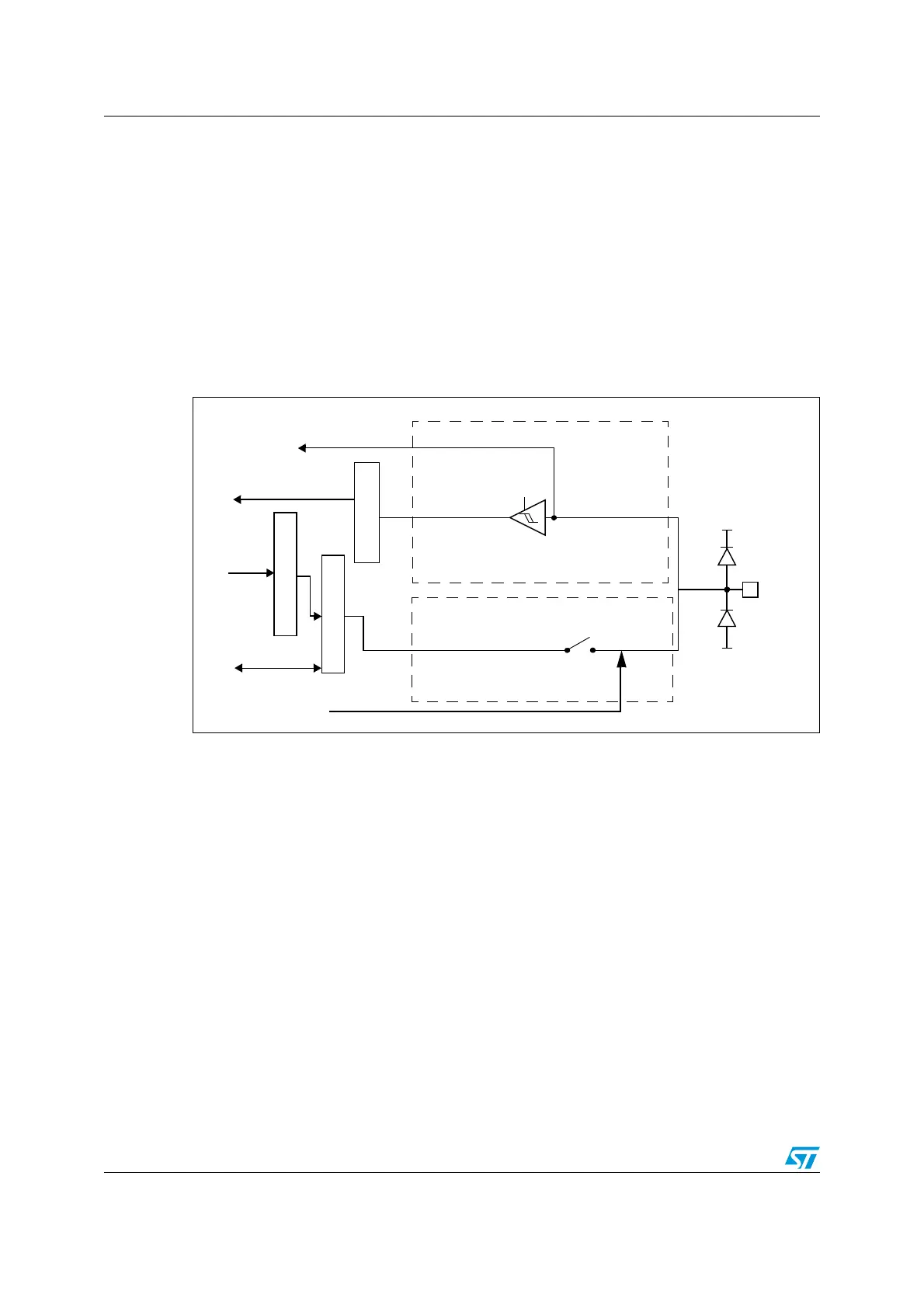
8.3.12 Analog configuration
When the I/O port is programmed as analog configuration:
● The output buffer is disabled
● The Schmitt trigger input is deactivated, providing zero consumption for every analog
value of the I/O pin. The output of the Schmitt trigger is forced to a constant value (0).
● The weak pull-up and pull-down resistors are disabled
● Read access to the input data register gets the value “0”
Note: In the analog configuration, the I/O pins cannot be 5 Volt tolerant.
Figure 17 shows the high-impedance, analog-input configuration of the I/O port bit.
Figure 17. High impedance-analog configuration
8.3.13 Using the HSE or LSE oscillator pins as GPIOs
When the HSE or LSE oscillator is switched OFF (default state after reset), the related
oscillator pins can be used as normal GPIOs.
When the HSE or LSE oscillator is switched ON (by setting the HSEON or LSEON bit in the
RCC_CSR register) the oscillator takes control of its associated pins and the GPIO
configuration of these pins has no effect.
When the oscillator is configured in a user external clock mode, only the OSC_IN or
OSC32_IN pin is reserved for clock input and the OSC_OUT or OSC32_OUT pin can still be
used as normal GPIO.
8.3.14 Using the GPIO pins in the backup supply domain
The PC13/PC14/PC15 GPIO functionality is lost when the core supply domain is powered
off (when the device enters Standby mode). In this case, if their GPIO configuration is not
bypassed by the RTC configuration, these pins are set in an analog input mode.
For details about I/O control by the RTC, refer to Section 24.3: RTC functional description on
page 536.
From on-chip
peripheral
To on-chip
peripheral
Analog
trigger
off
Input driver
0
Input data register
Output data register
Read/write
Read
Bit set/reset registers
Write
Analog
V
SS
V
DD
protection
diode
protection
diode
I/O pin