RM0091 Reset and clock control (RCC)
Doc ID 018940 Rev 1 85/742
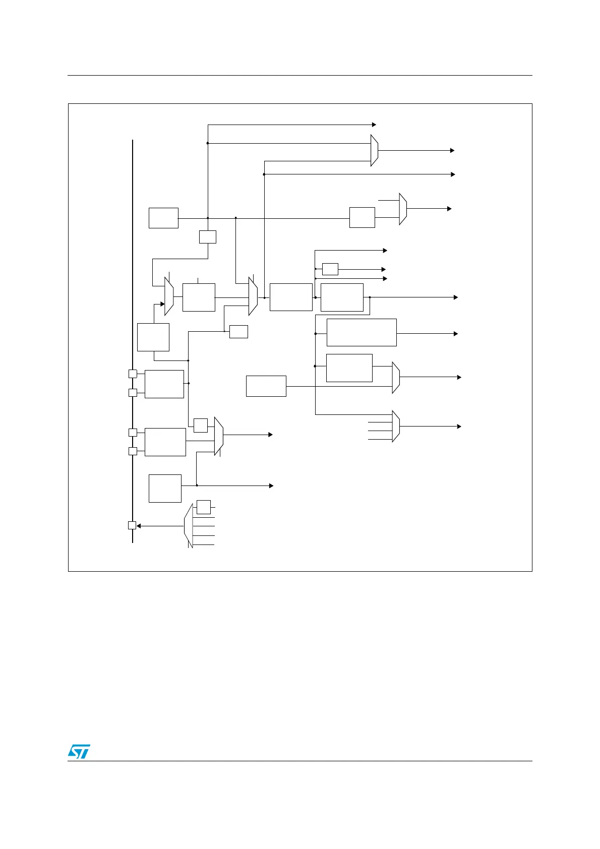
Figure 10. Clock tree
1. For full details about the internal and external clock source characteristics, please refer to the “Electrical characteristics”
section in your device datasheet.
/32
4-32 MHz
HSE OSC
OSC_IN
OSC_OUT
OSC32_IN
OSC32_OUT
8 MHz
HSI RC
to IWWDG
PLL
x2,x3,..
x16
PLLMUL
MCO
Main clock
output
AHB
/2
PLLCLK
HSI
HSE
APB
prescaler
/1,2,4,8,16
ADC
Prescaler
/2,4
HCLK
PLLCLK
to AHB bus, core,
memory and DMA
to ADC
14 MHz max
LSE
LSI
HSI
HSI
HSE
to RTC
PLLSRC
SW
MCO
/8
SYSCLK
RTCCLK
RTCSEL[1:0]
IWWDGCLK
SYSCLK
to TIM1,2,3,6,
14,15,16,17
If (APB1 prescaler
=1) x1 else x2
FLITFCLK
to Flash programming interface
HSI14
14 MHz
HSI14 RC
HSI14
/256
LSE
to I2C1
to USART1
LSE
HSI
SYSCLK
/2
PCLK
SYSCLK
HSI
PCLK
MS19935V1
to I2S1
to CEC
to cortex System timer
FHCLK Cortex free running clock
to APB peripherals
AHB
prescaler
/1,2,..512
CSS
/2,/3,...
/16
LSE OSC
32.768kHz
LSI RC
40kHz