Serial peripheral interface / inter-IC sound (SPI/I2S) RM0091
636/742 Doc ID 018940 Rev 1
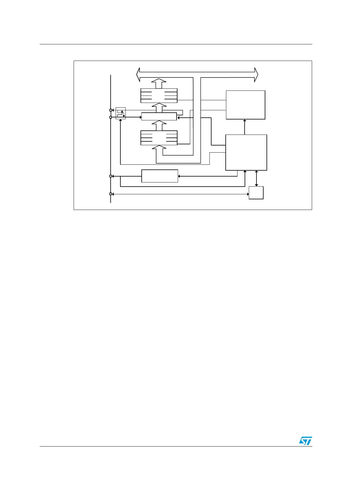
Figure 253. SPI block diagram
Four I/O pins are dedicated to SPI communication with external devices.
● MISO: Master In / Slave Out data. In the general case, this pin is used to transmit data
in slave mode and receive data in master mode.
● MOSI: Master Out / Slave In data. In the general case, this pin is used to transmit data
in master mode and receive data in slave mode.
● SCK: Serial Clock output pin for SPI masters and input pin for SPI slaves.
● NSS: Slave select pin. Depending on the SPI and NSS settings, this pin can be used to
either:
– select an individual slave device for communication
– synchronize the data frame or
– detect a conflict between multiple masters
See Section 26.3.4: Slave select (NSS) pin management for details.
The SPI bus allows the communication between one master device and one or more slave
devices. The bus consists of at least two wires - one for the clock signal and the other for
synchronous data transfer. Other signals can be added depending on the data exchange
between SPI nodes and their slave select signal management.
26.3.2 Communications between one master and one slave
The SPI allows the MCU to communicate using different configurations, depending on the
device targeted and the application requirements. These configurations use 2 or 3 wires
(with software NSS management) or 3 or 4 wires (with hardware NSS management).
Communication is always initiated by the master.
Full-duplex communication
By default, the SPI is configured for full-duplex communication. In this configuration, the shift
registers of the master and slave are linked using two unidirectional lines between the MOSI
MS30117 V1
Shift register
Write
Read
Baud rate
generator
Communication
controller
Address and data bus
CRC controller
NSS
logic
InternalNSS
BR[2 :0]
BIDIOE
CRCEN
CRCNEXT
CRCL
RXONLY
CPOL
CPHA
DS[0:3]
MOSI
MISO
SCK
NSS
Rx
FIFO
Tx
FIFO