General-purpose timers (TIM15/16/17) RM0091
394/742 Doc ID 018940 Rev 1
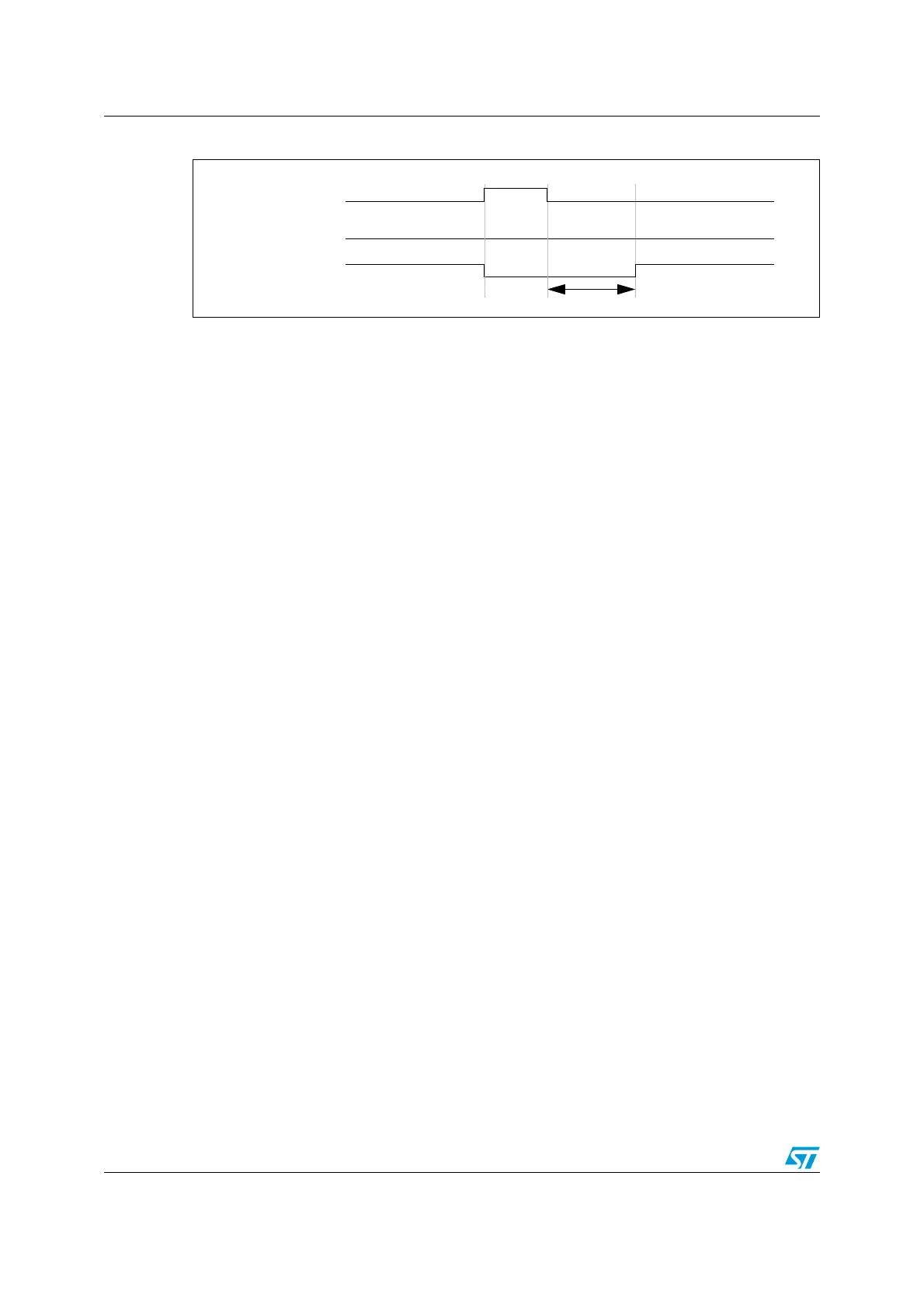
Figure 175. Dead-time waveforms with delay greater than the positive pulse.
The dead-time delay is the same for each of the channels and is programmable with the
DTG bits in the TIMx_BDTR register. Refer to Section 18.5.15: TIM15 break and dead-time
register (TIM15_BDTR) on page 417 for delay calculation.
Re-directing OCxREF to OCx or OCxN
In output mode (forced, output compare or PWM), OCxREF can be re-directed to the OCx
output or to OCxN output by configuring the CCxE and CCxNE bits in the TIMx_CCER
register.
This allows you to send a specific waveform (such as PWM or static active level) on one
output while the complementary remains at its inactive level. Other alternative possibilities
are to have both outputs at inactive level or both outputs active and complementary with
dead-time.
Note: When only OCxN is enabled (CCxE=0, CCxNE=1), it is not complemented and becomes
active as soon as OCxREF is high. For example, if CCxNP=0 then OCxN=OCxRef. On the
other hand, when both OCx and OCxN are enabled (CCxE=CCxNE=1) OCx becomes
active when OCxREF is high whereas OCxN is complemented and becomes active when
OCxREF is low.
18.4.12 Using the break function
When using the break function, the output enable signals and inactive levels are modified
according to additional control bits (MOE, OSSI and OSSR bits in the TIMx_BDTR register,
OISx and OISxN bits in the TIMx_CR2 register). In any case, the OCx and OCxN outputs
cannot be set both to active level at a given time. Refer to Table 54: Output control bits for
complementary OCx and OCxN channels with break feature on page 414 for more details.
The break source can be either the break input pin or a clock failure event, generated by the
Clock Security System (CSS), from the Reset Clock Controller. For further information on
the Clock Security System, refer to Section 7.2.7: Clock security system (CSS).
When exiting from reset, the break circuit is disabled and the MOE bit is low. You can enable
the break function by setting the BKE bit in the TIMx_BDTR register. The break input
polarity can be selected by configuring the BKP bit in the same register. BKE and BKP can
be modified at the same time. When the BKE and BKP bits are written, a delay of 1 APB
clock cycle is applied before the writing is effective. Consequently, it is necessary to wait 1
APB clock period to correctly read back the bit after the write operation.