RM0091 Embedded Flash memory
Doc ID 018940 Rev 1 53/742
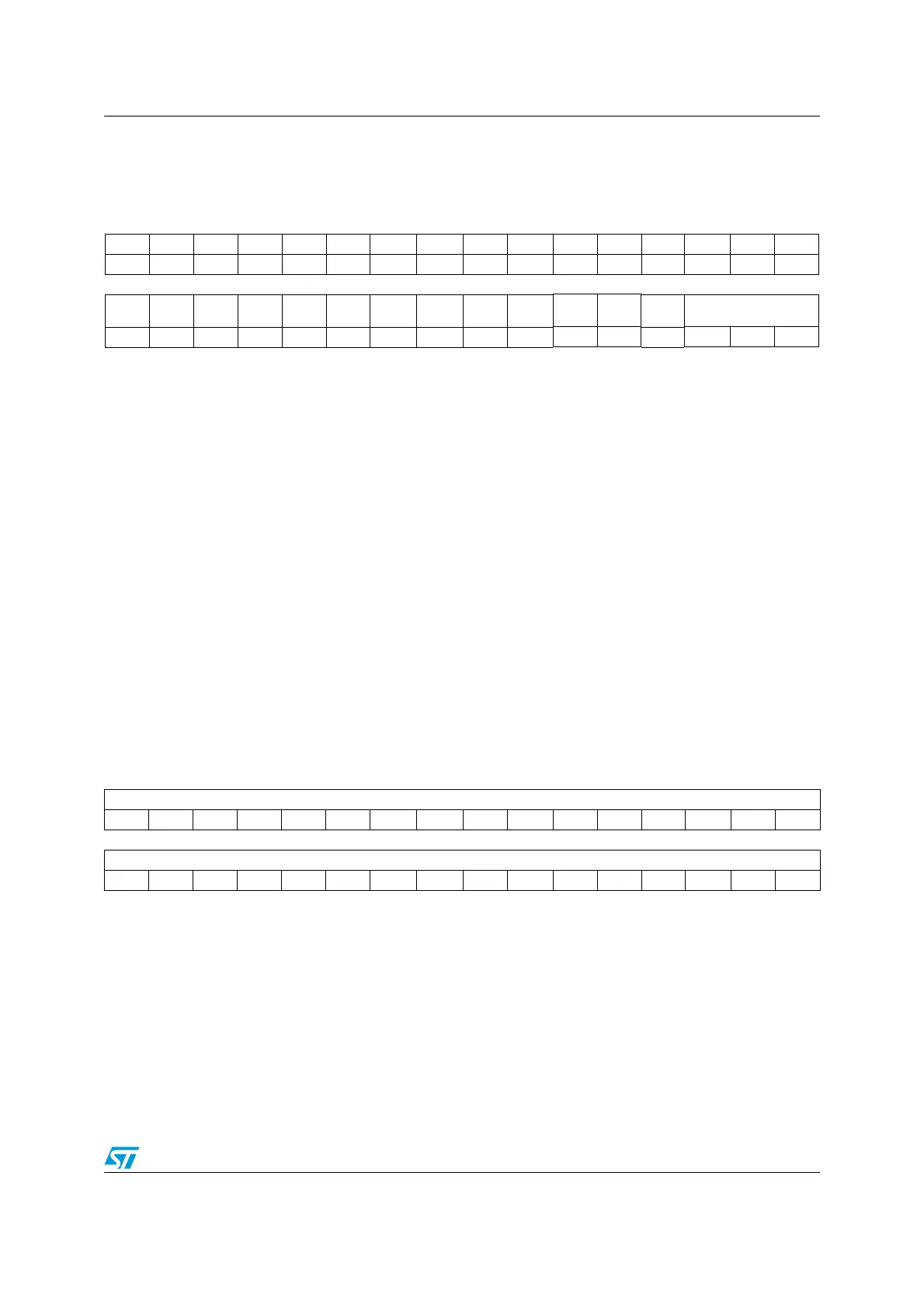
3.5.1 Flash access control register (FLASH_ACR)
Address offset: 0x00
Reset value: 0x0000 0000
3.5.2 Flash key register (FLASH_KEYR)
Address offset: 0x04
Reset value: xxxx xxxx
Note: These bits are all write-only and will return a 0 when read.
31 30 29 28 27 26 25 24 23 22 21 20 19 18 17 16
Res. Res. Res. Res. Res. Res. Res. Res. Res. Res. Res. Res. Res. Res. Res. Res.
15 14 13 12 11 10 9 8 7 6 5 4 3 2 1 0
Res. Res. Res. Res. Res. Res. Res. Res. Res. Res.
PRFT
BS
PRFT
BE
Res. LATENCY[2:0]
rrw rwrwrw
Bits 31:6 Reserved, must be kept at reset value.
Bit 5 PRFTBS: Prefetch buffer status
This bit provides the status of the prefetch buffer.
0: Prefetch buffer is disabled
1: Prefetch buffer is enabled
Bit 4 PRFTBE: Prefetch buffer enable
0: Prefetch is disabled
1: Prefetch is enabled
Bit 3 Reserved, must be kept at reset value.
Bits 1:0 LATENCY[2:0]: Latency
These bits represent the ratio of the SYSCLK (system clock) period to the Flash
access time.
000: Zero wait state, if 0 < SYSCLK≤ 24 MHz
001: One wait state, if 24 MHz < SYSCLK ≤ 48 MHz
31 30 29 28 27 26 25 24 23 22 21 20 19 18 17 16
FKEYR[31:16]
wwwwwww wwwwwwwww
15 14 13 12 11 10 9 8 7 6 5 4 3 2 1 0
FKEYR[15:0]
wwwwwww wwwwwwwww
Bits 31:0 FKEYR: Flash key
These bits represent the keys to unlock the Flash.