RM0091 Digital-to-analog converter (DAC1)
Doc ID 018940 Rev 1 207/742
Note: The ENx bit enables the analog DAC Channelx macrocell only. The DAC Channelx digital
interface is enabled even if the ENx bit is reset.
13.3.2 DAC output buffer enable
The DAC integrates an output buffer that can be used to reduce the output impedance, and
to drive external loads directly without having to add an external operational amplifier. The
DAC channel output buffer can be enabled and disabled using the BOFF1 bit in the
DAC_CR register.
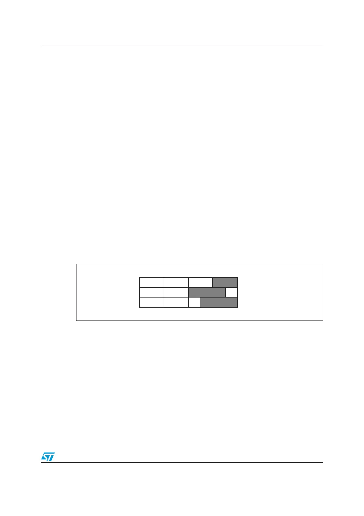
13.3.3 DAC data format
Depending on the selected configuration mode, the data have to be written into the specified
register as described below:
● There are three possibilities:
– 8-bit right alignment: the software has to load data into the DAC_DHR8Rx [7:0]
bits (stored into the DHRx[11:4] bits)
– 12-bit left alignment: the software has to load data into the DAC_DHR12Lx [15:4]
bits (stored into the DHRx[11:0] bits)
– 12-bit right alignment: the software has to load data into the DAC_DHR12Rx [11:0]
bits (stored into the DHRx[11:0] bits)
Depending on the loaded DAC_DHRyyyx register, the data written by the user is shifted and
stored into the corresponding DHRx (data holding registerx, which are internal non-
memory-mapped registers). The DHRx register is then loaded into the DORx register either
automatically, by software trigger or by an external event trigger.
Figure 39. Data registers in single DAC channel mode
13.3.4 DAC conversion
The DAC_DORx cannot be written directly and any data transfer to the DAC channelx must
be performed by loading the DAC_DHRx register (write to DAC_DHR8Rx, DAC_DHR12Lx,
DAC_DHR12Rx).
Data stored in the DAC_DHRx register are automatically transferred to the DAC_DORx
register after one APB1 clock cycle, if no hardware trigger is selected (TENx bit in DAC_CR
register is reset). However, when a hardware trigger is selected (TENx bit in DAC_CR
register is set) and a trigger occurs, the transfer is performed three PLCK1 clock cycles
later.
When DAC_DORx is loaded with the DAC_DHRx contents, the analog output voltage
becomes available after a time t
SETTLING
that depends on the power supply voltage and the
analog output load.
31 24 15 7 0
8-bit right aligned
12-bit left aligned
12-bit right aligned
ai14710