RM0091 Power control (PWR)
Doc ID 018940 Rev 1 77/742
6.4 Power control registers
The peripheral registers can be accessed by half-words (16-bit) or words (32-bit).
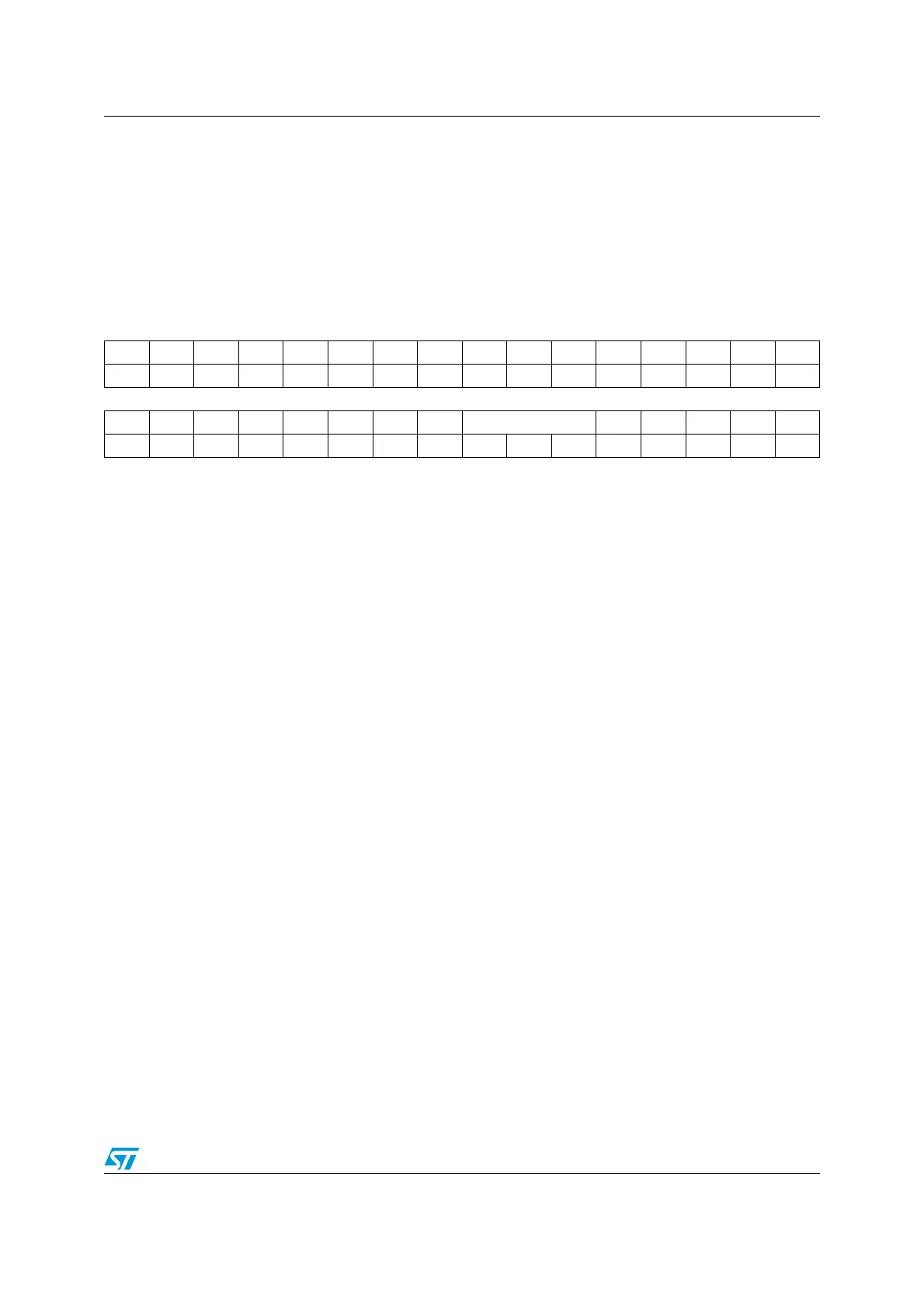
6.4.1 Power control register (PWR_CR)
Address offset: 0x00
Reset value: 0x0000 0000 (reset by wakeup from Standby mode)
31 30 29 28 27 26 25 24 23 22 21 20 19 18 17 16
Res Res Res Res Res Res Res Res Res Res Res Res Res Res Res Res
1514131211109876543210
Res Res Res Res Res Res Res DBP PLS[2:0] PVDE CSBF CWUF PDDS LPDS
rw rw rw rw rw rc_w1 rc_w1 rw rw
Bits 31:9 Reserved, must be kept at reset value..
Bit 8 DBP: Disable backup domain write protection.
In reset state, the RTC and backup registers are protected against parasitic write access.
This bit must be set to enable write access to these registers.
0: Access to RTC and Backup registers disabled
1: Access to RTC and Backup registers enabled
Bits 7:5 PLS[2:0]: PVD level selection.
These bits are written by software to select the voltage threshold detected by the Power
Voltage Detector.
Once the PVD_LOCK is enabled in the SYSCFG configuration register 2 (SYSCFG_CFGR2),
the PLS[2:0] bits cannot be programmed anymore.
000: PVD threshold 0
001: PVD threshold 1
010: PVD threshold 2
011: PVD threshold 3
100: PVD threshold 4
101: PVD threshold 5
110: PVD threshold 6
111: PVD threshold 7
Refer to the electrical characteristics of the datasheet for more details.
Bit 4 PVDE: Power voltage detector enable.
This bit is set and cleared by software. Once the PVD_LOCK is enabled in the SYSCFG
configuration register 2 (SYSCFG_CFGR2) register, the PVDE bit cannot be programmed
anymore.
0: PVD disabled
1: PVD enabled
Bit 3 CSBF: Clear standby flag.
This bit is always read as 0.
0: No effect
1: Clear the SBF Standby Flag (write).