Inter-integrated circuit (I
2
C) interface RM0091
470/742 Doc ID 018940 Rev 1
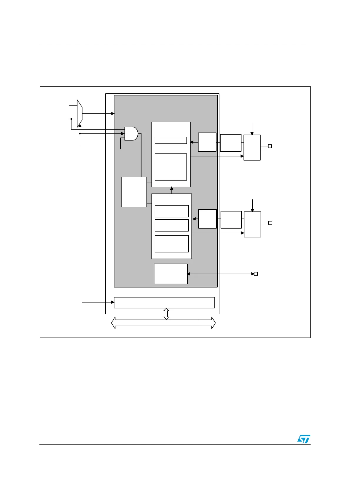
23.4.1 I2C1 block diagram
The block diagram of the I
2
C1 interface is shown in Figure 195.
Figure 195. I
2
C1 block diagram
The I2C1 is clocked by an independent clock source which allows to the I2C to operate
independently from the PCLK frequency.
This independent clock source can be selected for either of the following two clock sources:
● HSI: high speed internal oscillator (default value)
● SYSCLK: system clock
Refer to Reset and clock control (RCC) section for more details.
I2C1I/Os support 20 mA output current drive for Fast Mode Plus operation. This is enabled
by setting the driving capability control bits for SCL and SDA in the SYSCFG configuration
register 1 (SYSCFG_CFGR1) section.
MS19873V2
HSI
SYSCLK
WUPEN
RCC_I2C1SW
(from reset and
clock
controller)
I2CCLK
Wakeup
on
address
match
SMBUS
PEC
generation/
check
Shift register
Data control
SMBus
Timeout
check
Clock control
Master clock
generation
Slave clock
stretching
SMBus Alert
control &
status
Digital
noise
filter
I2C1_SCL
From system configuration
controller (SYSCFG)
FM+ drive
I2C1_SMBA
PCLK
Registers
APB bus
GPIO
logic
Analog
noise
filter
Digital
noise
filter
I2C1_SDA
From system configuration
controller (SYSCFG)
FM+ drive
GPIO
logic
Analog
noise
filter