RM0091 Serial peripheral interface / inter-IC sound (SPI/I2S)
Doc ID 018940 Rev 1 641/742
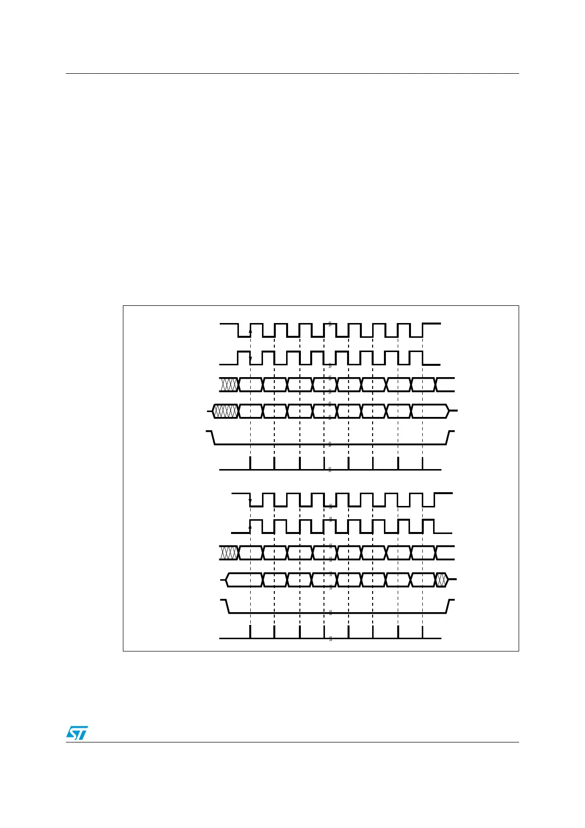
CPOL is reset, the SCK pin has a low-level idle state. If CPOL is set, the SCK pin has a
high-level idle state.
If the CPHA bit is set, the second edge on the SCK pin is the first MSBit capture strobe
(falling edge if the CPOL bit is reset, rising edge if the CPOL bit is set). Data are latched on
each occurrence of this clock transition type. If the CPHA bit is reset, the first edge on the
SCK pin is the first MSBit capture strobe (falling edge if the CPOL bit is set, rising edge if the
CPOL bit is reset). Data are latched on each occurrence of this clock transition type.
The combination of CPOL (clock polarity) and CPHA (clock phase) bits selects the data
capture clock edge.
Figure 259, shows an SPI full-duplex transfer with the four combinations of the CPHA and
CPOL bits.
Note: Prior to changing the CPOL/CPHA bits the SPI must be disabled by resetting the SPE bit.
The idle state of SCK must correspond to the polarity selected in the SPIx_CR1 register (by
pulling up SCK if CPOL=1 or pulling down SCK if CPOL=0).
Figure 259. Data clock timing diagram
1. These timings are shown with the LSBFIRST bit reset in the SPIx_CR1 register and 8-bit data size (bits
DS[3:0]=0111).
CPOL = 1
CPOL = 0
MSBit
LSBit
MSBit
LSBit
MISO
MOSI
NSS
(to slave)
Capture strobe
CPHA =1
CPOL = 1
CPOL = 0
MSBit
LSBit
MSBit
LSBit
MISO
MOSI
NSS
(to slave)
Capture strobe
CPHA =0
ai17154c