RM0091 General-purpose I/Os (GPIO)
Doc ID 018940 Rev 1 119/742
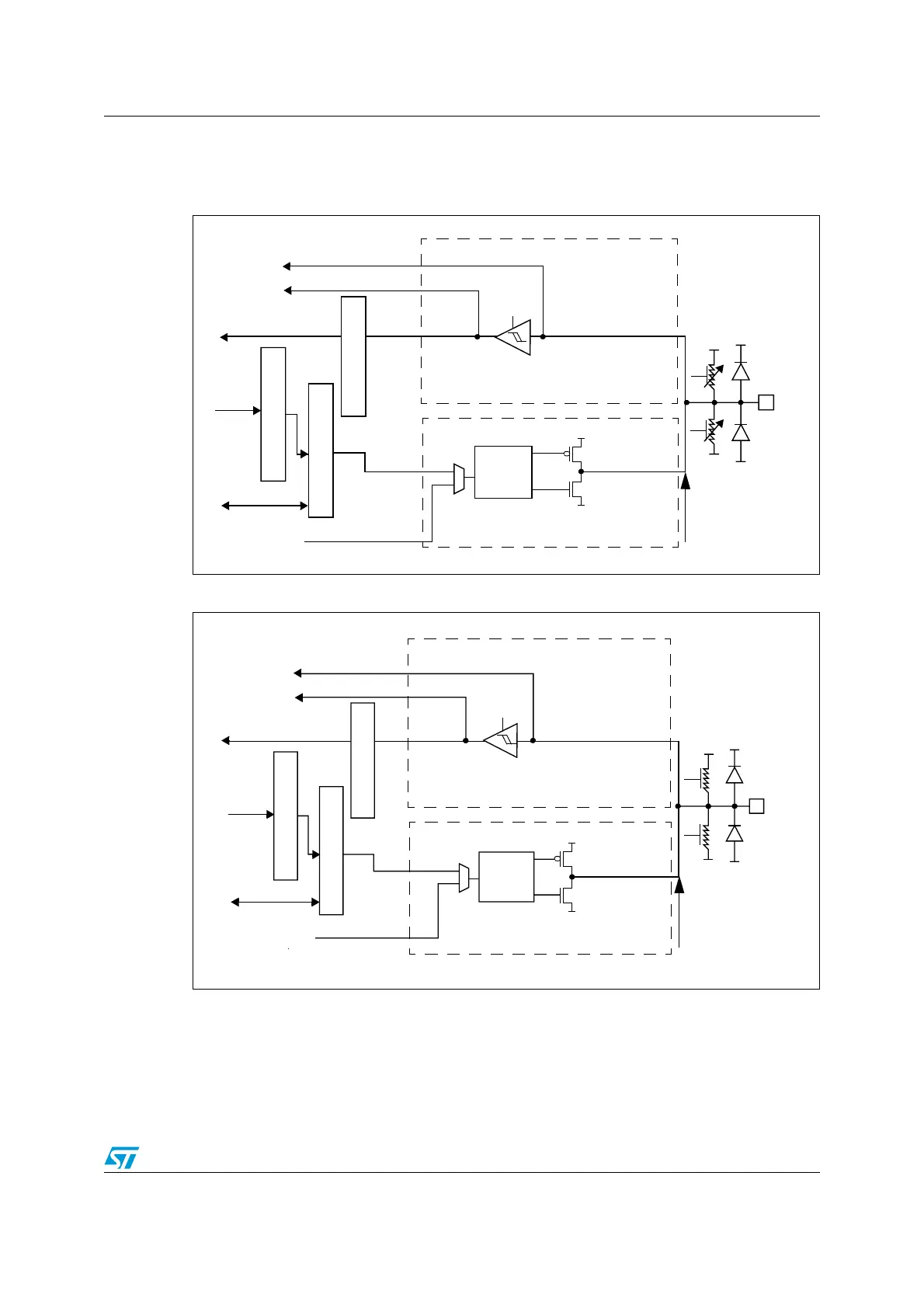
Figure 12 and Figure 13 show the basic structures of a standard and a 5 V tolerant I/O port
bit, respectively. Tabl e 2 1 gives the possible port bit configurations.
Figure 12. Basic structure of a standard I/O port bit
Figure 13. Basic structure of a five-volt tolerant I/O port bit
1. V
DD_FT
is a potential specific to five-volt tolerant I/Os and different from V
DD
.
Alternate function output
Alternate function input
Push-pull,
open-drain or
disabled
Input data register
Output data register
Read/write
From on-chip
peripheral
To on-chip
peripheral
Output
control
Analog
on/off
Pull
Pull
down
on/off
I/O pin
V
DD
V
DD
V
SS
V
SS
trigger
V
SS
V
DD
Protection
diode
Protection
diode
on/off
Input driver
Output driver
up
P-MOS
N-MOS
Read
Bit set/reset registers
Write
Analog
ai15938
Alternate function output
Alternate function input
Push-pull,
open-drain or
disabled
Output data register
Read/write
From on-chip
peripheral
To on-chip
peripheral
Output
control
Analog
on/off
Pull
Pull
on/off
I/O pin
V
DD
V
DD
V
SS
V
SS
TTL Schmitt
trigger
V
SS
V
DD_FT
(1)
Protection
diode
Protection
diode
on/off
Input driver
Output driver
down
up
P-MOS
N-MOS
Read
Bit set/reset registers
Write
Analog
Input data register
ai15939b