RM0091 Serial peripheral interface / inter-IC sound (SPI/I2S)
Doc ID 018940 Rev 1 645/742
The correct disable procedure for certain receive only modes is:
1. Disable receive only mode in the specific time window while the last data frame is
ongoing (RXONLY=0 or BIDIOE = 1)
2. Wait until BSY=0 (the last data frame is processed).
3. Read data until FRLVL[1:0] = 00 (read all the received data)
4. Disable the SPI (SPE=0).
Note: If packing mode is used and an odd number of data frames with a format less than or equal
to 8 bits (fitting into one byte) has to be received, FRXTH must be set when FRLVL[1:0] =
01, in order to generate the RXNE event to read the last odd data frame.
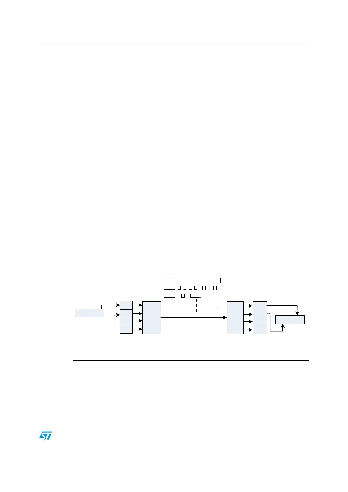
Data packing
When the data frame size fits into one byte (less than or equal to 8 bits), data packing is
used automatically when any read or write 16-bit access is performed on the SPIx_DR
register. The double data frame pattern is handled in parallel in this case. At first, the SPI
operates using the pattern stored in the LSB of the accessed word, then with the other half
stored in the MSB. Figure 261 provides an example of data packing mode sequence
handling. Two data frames are sent after the single 16-bit access the SPIx_DR register of
the transmitter. This sequence can generate just one RXNE event in the receiver if the
RXFIFO threshold is set to 16 bits (FRXTH=0). The receiver then has to access both data
frames by a single 16-bit read of SPIx_DR as a response to this single RXNE event. The
RxFIFO threshold setting and the following read access must be always kept aligned at the
receiver side, as data can be lost if it is not in line.
A specific problem appears if an odd number of such “fit into one byte” data frames must be
handled. On the transmitter side, writing the last data frame of any odd sequence with an 8-
bit access to SPIx_DR is enough. The receiver has to change the Rx_FIFO threshold level
for the last data frame received in the odd sequence of frames in order to generate the
RXNE event.
Figure 261. Packing data in FIFO for transmission and reception
0x04
0x0A
SPI fsm
& shift
TXFIFO
SPIx_DR
0x0A
0x04
0x0A 0x04
SPI fsm
& shift
0x0A
0x04
0x04
0x0A
SPIx_DR
16-bit access when write to data register
SPI_DR= 0x040A when TxE=1
16-bit access when read from data register
SPI_DR= 0x040A when RxNE=1
NSS
SCK
MOSI
RXFIFO
MS19590V1