RM0091 Serial peripheral interface / inter-IC sound (SPI/I2S)
Doc ID 018940 Rev 1 653/742
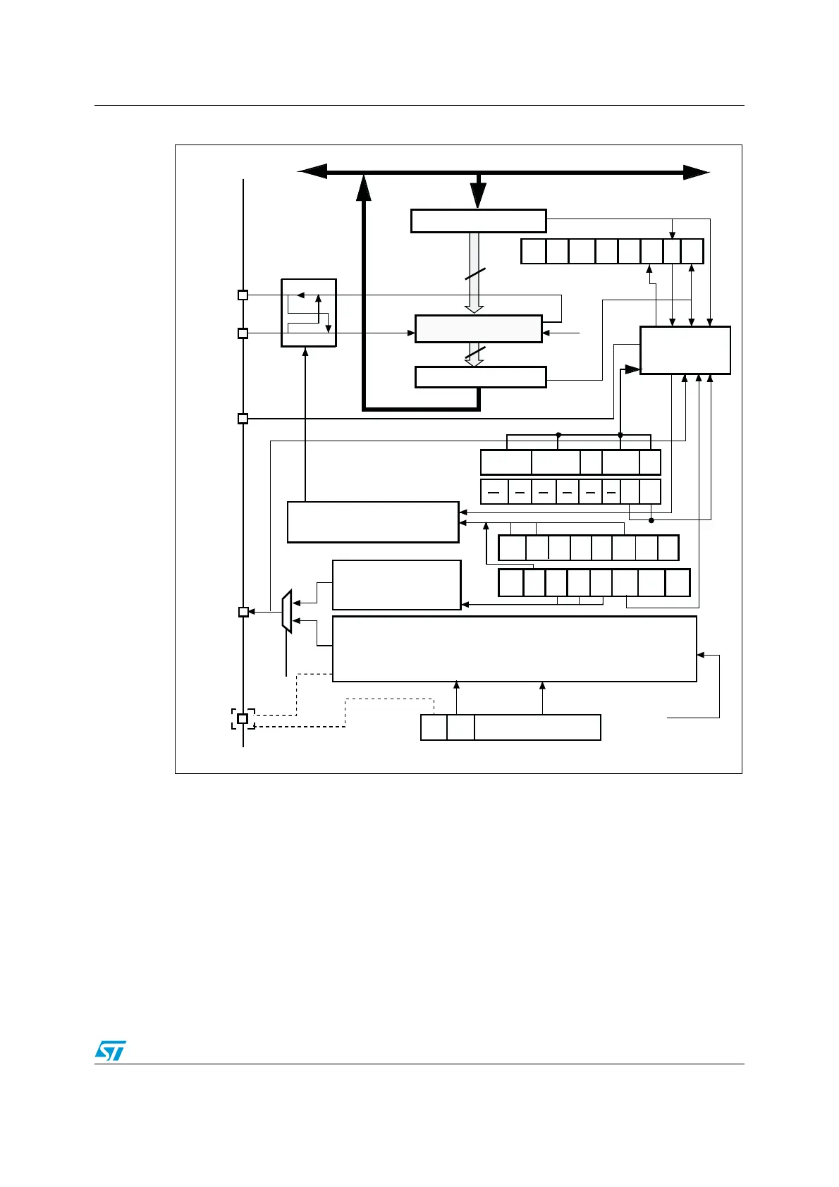
Figure 264. I
2
S block diagram
1. The MISO pin is not used in I
2
S mode.
The SPI can function as an audio I
2
S interface when the I
2
S capability is enabled (by setting
the I2SMOD bit in the SPIx_I2SCFGR register). This interface mainly uses the same pins,
flags and interrupts as the SPI.
The I
2
S shares three common pins with the SPI:
● SD: Serial Data (mapped on the MOSI pin) to transmit or receive the two time-
multiplexed data channels (in simplex mode only).
● WS: Word Select (mapped on the NSS pin) is the data control signal output in master
mode and input in slave mode.
● CK: Serial Clock (mapped on the SCK pin) is the serial clock output in master mode
and serial clock input in slave mode.
Tx buffer
Shift register
16-bit
Communication
Rx buffer
16-bit
MOSI/ SD
Master control logic
MISO
SPI
baud rate generator
CK
I2SMOD
LSB first
LSB
First
SPE BR2 BR1 BR0
MSTR CPOL CPHA
Bidi
mode
Bidi
OE
CRC
EN
CRC
Next
DFF
Rx
only
SSM
SSI
Address and data bus
control
NSS/WS
BSY OVR MODF
CRC
ERR
CH
SIDE
TxE RxNE
I
2
S clock generator
MCK
I2S_CK
I2S
MOD
I2SE
CH
DATLEN
LEN
CKPOL
I2SCFG I2SSTD
MCKOE ODD I2SDIV[7:0]
[1:0] [1:0] [1:0]
UDR
I2SxCLK
ai14748