Advanced-control timers (TIM1) RM0091
288/742 Doc ID 018940 Rev 1
15.4.19 TIM1 DMA control register (TIM1_DCR)
Address offset: 0x48
Reset value: 0x0000
Bits 7:0 DTG[7:0]: Dead-time generator setup
This bit-field defines the duration of the dead-time inserted between the complementary
outputs. DT correspond to this duration.
DTG[7:5]=0xx => DT=DTG[7:0]x t
dtg
with t
dtg
=t
DTS
.
DTG[7:5]=10x => DT=(64+DTG[5:0])xt
dtg
with T
dtg
=2xt
DTS
.
DTG[7:5]=110 => DT=(32+DTG[4:0])xt
dtg
with T
dtg
=8xt
DTS
.
DTG[7:5]=111 => DT=(32+DTG[4:0])xt
dtg
with T
dtg
=16xt
DTS
.
Example if T
DTS
=125 ns (8 MHz), dead-time possible values are:
0 to 15875 ns by 125 ns steps,
16 us to 31750 ns by 250 ns steps,
32 us to 63 us by 1 us steps,
64 us to 126 us by 2 us steps
Note: This bit-field can not be modified as long as LOCK level 1, 2 or 3 has been programmed
(LOCK bits in TIMx_BDTR register).
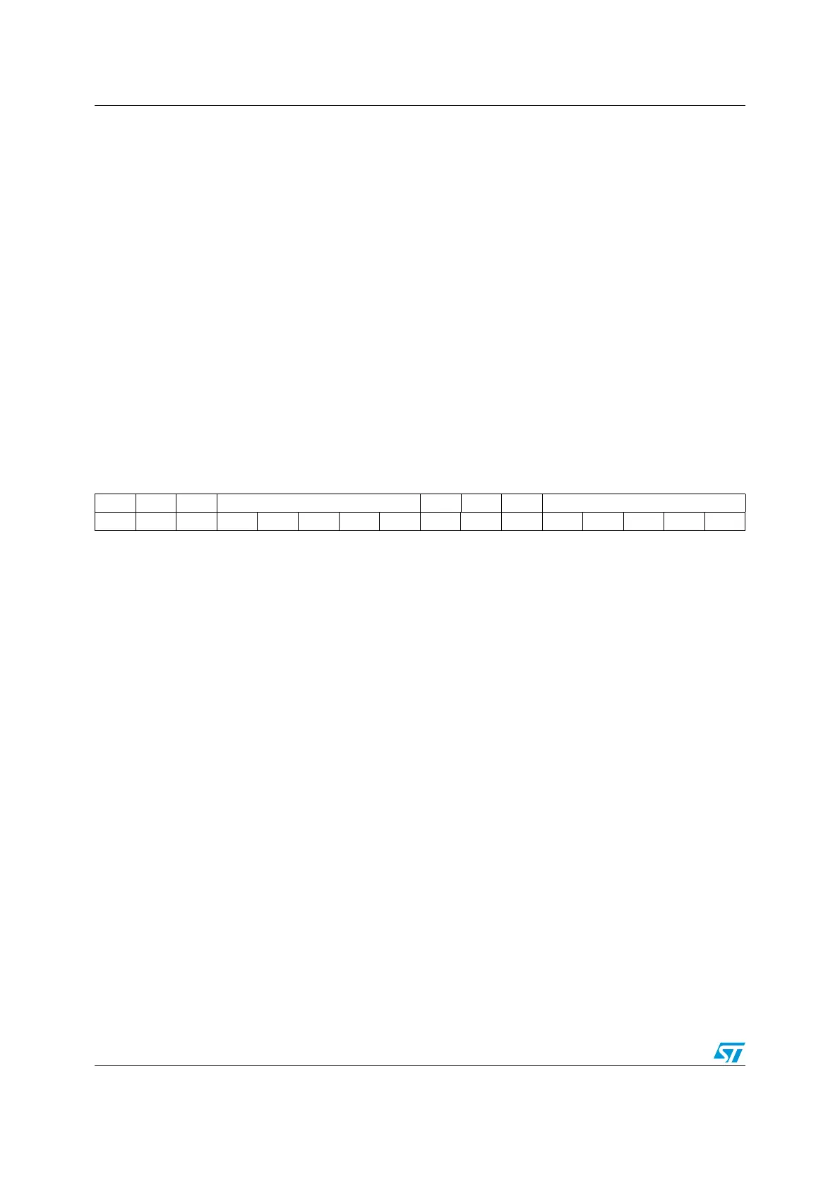
1514131211109876543210
Res. Res. Res. DBL[4:0] Res. Res. Res. DBA[4:0]
rw rw rw rw rw rw rw rw rw rw
Bits 15:13 Reserved, must be kept at reset value.
Bits 12:8 DBL[4:0]: DMA burst length
This 5-bit vector defines the number of DMA transfers (the timer recognizes a burst transfer
when a read or a write access is done t
the TIMx_DMAR address)
00000: 1 transfer
00001: 2 transfers
00010: 3 transfers
...
10001: 18 transfers
Bits 7:5 Reserved, must be kept at reset value.
Bits 4:0 DBA[4:0]: DMA base address
This 5-bit vector defines the base-address for DMA transfers (when read/write access are
done through the TIMx_DMAR address). DBA is defined as an offset starting from the
address of the TIMx_CR1 register.
Example:
00000: TIMx_CR1,
00001: TIMx_CR2,
00010: TIMx_SMCR,
...
Example: Let us consider the following transfer: DBL = 7 transfers and DBA = TIMx_CR1. In
this case the transfer is done to/from 7 registers starting from the TIMx_CR1 address.