RM0091
40/742 Doc ID 018940 Rev 1
2.3 Embedded SRAM
The STM32F05xxx features up to 8 Kbytes of static SRAM. It can be accessed as bytes,
half-words (16 bits) or full words (32 bits). This memory can be addressed at maximum
system clock frequency without wait state and thus by both CPU and DMA.
Parity check
The user can enable the parity check using the option bit RAM_PARITY_CHECK in the user
option byte (refer to Table 11 on page 60).
The data bus width is 36 bits because 4 bits are available for parity check (1 bit per byte) in
order to increase memory robustness, as required for instance by Class B or SIL norms.
The parity bits are computed and stored when writing into the SRAM. Then, they are
automatically checked when reading. If one bit fails, an NMI is generated. The same error
can also be linked to the BRK_IN Break input of TIMER15/TIM16/TIM7, with the
SRAM_PARITY_LOCK control bit in the SYSCFG configuration register 2
(SYSCFG_CFGR2). The SRAM Parity Error flag (SRAM_PEF) is available in the SYSCFG
configuration register 2 (SYSCFG_CFGR2).
2.4 Flash memory overview
The Flash memory is composed of two distinct physical areas:
● The main Flash memory block. It contains the application program and user data if
necessary.
● The information block. It is composed of two parts:
– Option bytes for hardware and memory protection user configuration.
– System memory which contains the proprietary boot loader code.
Please, refer to Section 3: Embedded Flash memory for more details.
The Flash interface implements instruction access and data access based on the AHB
protocol. It implements the prefetch buffer that speeds up CPU code execution. It also
implements the logic necessary to carry out the Flash memory operations (Program/Erase)
controlled through the Flash registers.
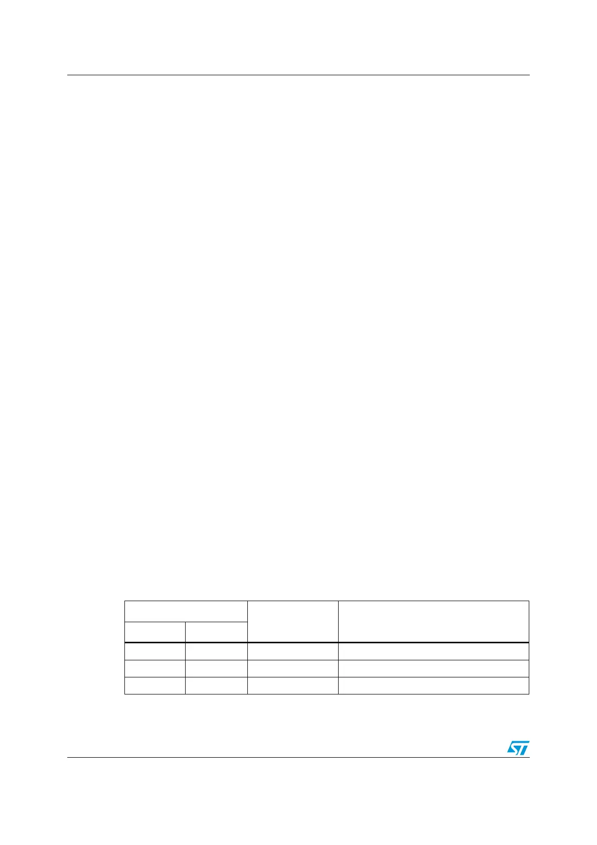
2.5 Boot configuration
In the STM32F05xxx, three different boot modes can be selected through the BOOT0 pin
and nBOOT1 bit in in the User option byte, as shown in the following table.
Table 3. Boot modes
Boot mode selection
Boot mode Aliasing
BOOT1 BOOT0
x 0 Main Flash memory Main Flash memory is selected as boot space
0 1 System memory System memory is selected as boot space
1 1 Embedded SRAM Embedded SRAM is selected as boot space