System Interface Unit (SIU)
MPC5553/MPC5554 Microcontroller Reference Manual, Rev. 5
6-92 Freescale Semiconductor
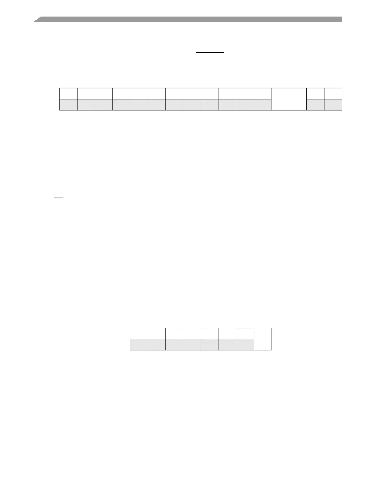
6.3.1.12.116 Pad Configuration Register 230 (SIU_PCR230)
The SIU_PCR230 register controls the slew rate of the RSTOUT pin.
Figure 6-128. RSTOUT Pad Configuration Register (SIU_PCR230)
Refer to Table 6-16 for bit field definitions.
6.3.1.13 GPIO Pin Data Output Registers 0–213 (SIU_GPDOn)
The definition of the 8-bit SIU_GPDOn registers, with each register specifying the drive data for a single
GPIO pin, is given in Figure 6-129. The n notation in the name of the 214 SIU_GPDOn registers
corresponds to the pins with the same GPIO pin numbers. For example, PDO0 is the pin data output bit
for the CS[0]_GPIO[0] pin and is found in SIU_GPDO0, and PDO213 is the pin data output bit for the
WKPCFG_GPIO[213] pin and is found in SIU_GPDO213. The GPDO address for a particular pin is equal
to the GPIO pin number with an offset of SIU_BASE + 0x0600.
The SIU_GPDOn registers are written to by software to drive data out on the external GPIO pin. Each
register drives a single external GPIO pin, which allows the state of the pin to be controlled independently
from other GPIO pins. Writes to the SIU_GPDOn registers have no effect on pin states if the pins are
configured as inputs by the associated pad configuration registers. The SIU_GPDO[n] register values are
automatically driven to the GPIO pins without software update if the direction of the GPIO pins is changed
from input to output.
Writes to the SIU_GPDOn registers have no effect on the state of the corresponding pins when the pins
are configured for their primary function by the corresponding PCR.
Address: Base + 0x020C Access: Read / write[12:13]
0123456789101112131415
R 000000000000
SRC
00
W
RESET: 0000000000001100
Address: Base + 0x0600 + n Access: Read / write[7]
01234567
R
00000000
W
PDOn
Reset
00000000
Figure 6-129. GPIO Pin Data Output Register 0–213 (SIU_GPDOn)