System Interface Unit (SIU)
MPC5553/MPC5554 Microcontroller Reference Manual, Rev. 5
Freescale Semiconductor 6-93
6.3.1.14 GPIO Pin Data Input Registers 0–213 (SIU_GPDIn)
The definition of the 8-bit SIU_GPDIn registers, with each register specifying the drive data for a single
GPIO pin, is given in Figure 6-130. The n notation in the name of the 178 (MPC5553) or 214 (MPC5554)
SIU_GPDIn registers corresponds to the pins with the same GPIO pin numbers. For example, PDI0 is the
bit for the CS[0]_GPIO[0] data input pin and is set in SIU_GPDI0; PDI213 is the bit for the data input
WKPCFG_GPIO[213] pin and is found in SIU_GPDI213. The GPDI address for a pin is the GPIO pin
number with an offset of SIU_BASE + 0x0800. Gaps exist in the SIU memory where the pin is not
available in the package.
The SIU_GPDIn registers are read-only registers that allow software to read the input state of an external
GPIO pin. Each register represents the input state of a single external GPIO pin. If the GPIO pin is
configured as an output, and the input buffer enable (IBE) bit is set in the PCR register, the SIU_GPDIn
register contains the state of the output pin.
6.3.1.15 eQADC Trigger Input Select Register (SIU_ETISR)
The SIU_ETISR selects the source for the eQADC trigger inputs. The eQADC trigger numbers 0–5
specified by TSEL(0–5) correspond to CFIFO numbers 0–5. To calculate the CFIFO number to which each
trigger is connected, divide the DMA channel number by two. For example, eQADC CFIFO 1 (connected
to DMA channel 2) can be triggered by eTPUA[31], eMIOS[11] or ETRIG[1]. To select a trigger, the
TSEL must be initialized.
Table 6-45. SIU_GPDOn Field Descriptions
Field Name Description
PDOn
Pin data out. Stores the data to be driven out on the external GPIO pin associated
with the register. If the register is read, it returns the value written.
0V
OL
is driven on the external GPIO pin when the pin is configured as an output.
1V
OH
is driven on the external GPIO pin when the pin is configured as an output.
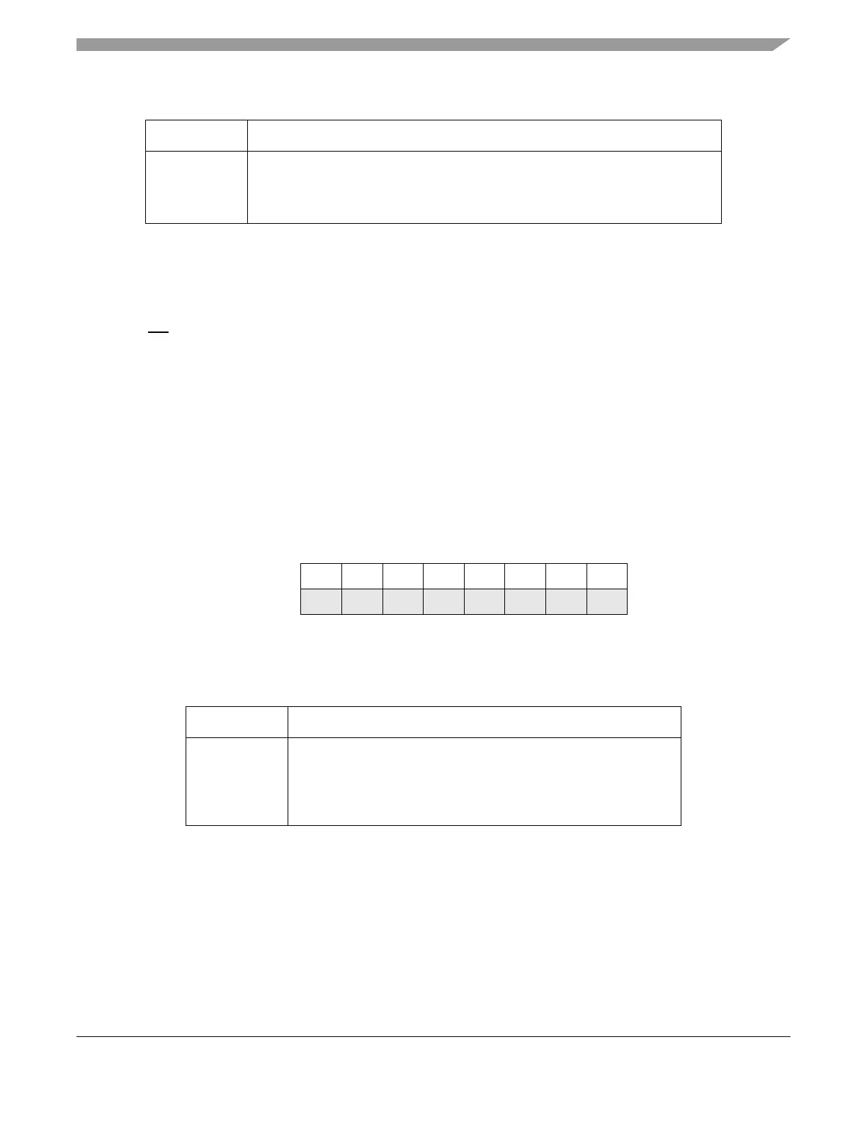
Address: Base + 0x0800 + n Access: Read Only [7]
01234567
R
0000000PDIn
W
Reset
00000000
Figure 6-130. GPIO Pin Data Input Register 0–213 (SIU_GPDIn)
Table 6-46. SIU_GPDIn Field Description
Field Name Description
PDIn
Input pin. This bit reflects the input state on the external GPIO pin
associated with the register.
If PCRn[IBE] = 1, then:
0 Signal on pin is less than or equal to V
IL
.
1 Signal on pin is greater than or equal to V
IH
.