MPC5553/MPC5554 Microcontroller Reference Manual, Rev. 5
17-46 Freescale Semiconductor
In order to achieve a duty cycle of 100%, both registers A1 and B1 must be set to the same value. When a
simultaneous match occurs between the selected time base and registers A1 and B1, the output flip-flop is
set at every period to the value of EDPOL bit and the selected time base switches to the selected counter
bus, allowing a new cycle to begin at any time, as previously described. 0% duty cycle is possible by
writing 0x000000 to register A. When a match occurs, the output flip-flop is set at every period to the
complement of EDPOL bit and the selected time base switches to the selected counter bus, allowing a new
cycle to begin at any time, as previously described. In both cases, FLAG is generated regardless of
MODE[5] bit.
NOTE
If A1 and B1 are set to the 0x000000, a 0% duty cycle waveform is
produced.
NOTE
Any updates to the A or B register will take place immediately.
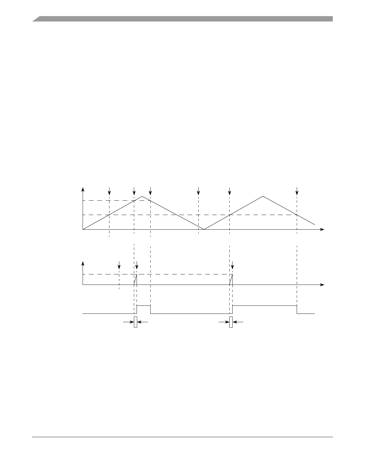
Figure 17-33 and Figure 17-34 show the unified channel running in OPWMC with leading and trailing
dead time, respectively.
Figure 17-33. Output PWMC with Leading Dead-time Insertion
Output
Flip-Flop
A1 Match A1 Match
Time
0x000000
0x000303
0x000200
Update to
A1
Selected
MODE[6] = 1
Counter Bus
A1 Match
Notes:
1
Writing EMIOS_An writes to A2.
2
Writing EMIOS_Bn writes to B1.
A2value transferred to A1 according to OUn bit.
B2value transferred to B1 according to OUn bit.
Update to
A1
A1 Match
A1 Value
1
$000200$000200
0x000303 0x000303
0x000200
0x000303
0xxxxxxx
Update to
B1
B1 Match
0x000010
0x000000
EMIOS_CCNTR
B1
Match
B1 Value
2
0x000010
Time