MPC5553/MPC5554 Microcontroller Reference Manual, Rev. 5
17-48 Freescale Semiconductor
The value loaded in register A1 is compared with the value on the selected time base. When a match on
comparator A occurs, the output flip-flop is set to the value of the EDPOL bit. When a match occurs on
comparator B, the output flip-flop is set to the complement of the EDPOL bit.
FLAG can be generated at match B, when MODE[5] is cleared, or in both matches, when MODE[5] is set.
At any time, the FORCMA and FORCMB bits allow the software to force the output flip-flop to the level
corresponding to a match on A or B respectively. Note that FLAG bit is not set by the FORCMA and
FORCMB operations.
If subsequent matches occur on comparators A and B, the PWM pulses continue to be generated,
regardless of the state of the FLAG bit.
In order to achieve 0% duty cycle, both registers A1 and B1 must be set to the same value. When a
simultaneous match on comparators A and B occur, the output flip-flop is set at every period to the value
of EDPOL bit. 0% duty cycle is possible by writing 0x000000 to register A. When a match occurs, the
output flip-flop is set at every period to the complement of EDPOL bit. The transfer from register B2 to
B1 is still controlled by MODE[6] bit.
NOTE
If A1 and B1 are set to the 0x000000, a 100% duty cycle waveform is
produced.
NOTE
Updates to the A register will always occur immediately. If next period
update is selected via the mode[6] bit, only the B register update is delayed
until the next period.
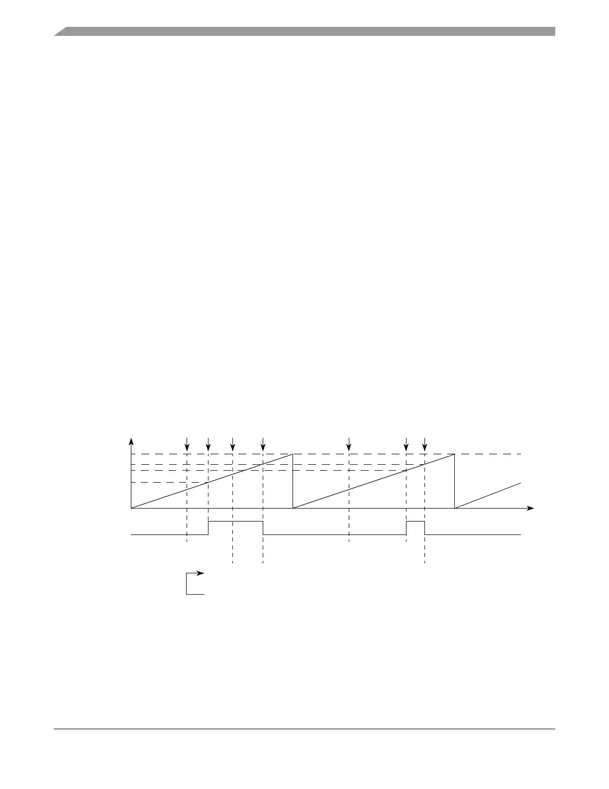
Figure 17-35 and Figure 17-36 show the unified channel running in OPWM with immediate update and
next period update, respectively.
Figure 17-35. Output PWM with Immediate Update
A1 Value1
B1 Value
B2 Value2
0x001000
Output
Flip-Flop
Time
0x000000
B1 Match
0x0009000x000900
0xFFFFFF
0x001000
0x000900
Update to
A1
0xxxxxxx0x000200
Update to
A1
0x001000
Selected
MODE[6] = 0
Counter Bus
A1 Match B1 Match
0xxxxxxx
0xxxxxxx
0x001000
Notes: 1 Writing EMIOS_An writes to A2.
2 Writing EMIOS_Bn writes to B2.
A2value transferred to A1 according to OUn bit.
B2value transferred to B1 according to OUn bit.
0x000200
Write to
B2
A1
Match
0x001000