MPC5553/MPC5554 Microcontroller Reference Manual, Rev. 5
Freescale Semiconductor 17-55
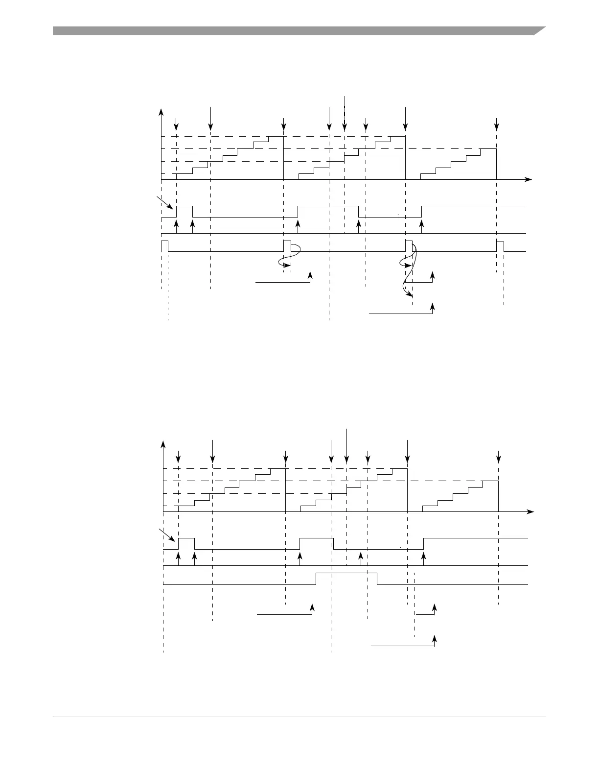
Figure 17-43. eMIOS OPWFMB Mode Example — A1/B1 Updates and Flags
Figure 17-44 shows the operation of the output disable feature in OPWFMB mode. Unlike OPWFM mode,
the output disable forces the channel output flip-flop to the EDPOL bit value. This functionality targets
applications that use active high signals and a high to low transition at A1 match. For such cases EDPOL
should be 0.
Figure 17-44. eMIOS OPWFMB Mode Example — Active Output Disable
Cycle n Cycle n+1 Cycle n+2
A1 Value
B1 Value
B2 Value
0x000008
0x000002
0x000006
0x000008
0x000001
0x000004
0x000006
MODE[0] = 1
A2 Value
0x000002 0x000004 0x000006
0x000002
0x000004
0x000006
0x000008 0x000006
Output Flip-Flop
Write to B2
Match A1 Match B1
Match B1
A1/B1 Load Signal
Due to B1 Match
FLAG Set Event
Cycle n-1
Time
Write to A2
Match A1
Write to A2 Match B1
EDPOL = 0
EMIOS_CCNTRn