GD32F3x0 User Manual
154
4. Confi gure the PRIO bits in the DMA_CHxCTL register to set the channel software
priority.
5. Configure the memory and peripheral transfer width, memory and peripheral address
generation algorithm in the DMA_CHxCTL register.
6. Configure the enable bit for full transfer finish interrupt, half transfer finish interrupt,
transfer error interrupt in the DMA_CHxCTL register.
7. Configure the DMA_CHxPADDR register for setting the peripheral base address.
8. Configure the DMA_CHxMADDR register for setting the memory base address.
9. Configure the DMA_CHxCNT register to set the total transfer data number.
10. Configure the CHEN bit with ‘1’ in the DMA_CHxCTL register to enable the channel.
9.4.8. Interrupt
Each DMA channel has a dedicated interrupt. There are three types of interrupt event,
including full transfer finish, half transfer finish, and transfer error.
Each interrupt event has a dedicated flag bit in the DMA_INTF register, a dedicated clear bit
in the DMA_INTC register, and a dedicated enable bit in the DMA_CHxCTL register. The
relationship is described in the following Table 9-2. interrupt events.
Table 9-2. interrupt events
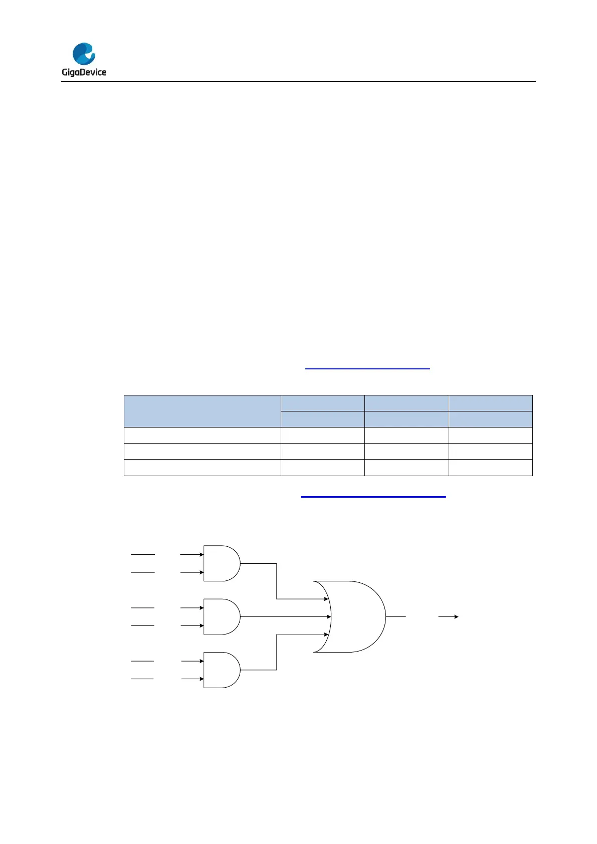
The DMA interrupt logic is shown in the Figure 9-3. DMA interrupt logic, an interrupt can be
produced when any type of interrupt event occurs and enabled on the channel.
Figure 9-3. DMA interrupt logic
 Loading...

