GD32F3x0 User Manual
78
4.3. Register definition
RCU base address: 0x4002 1000
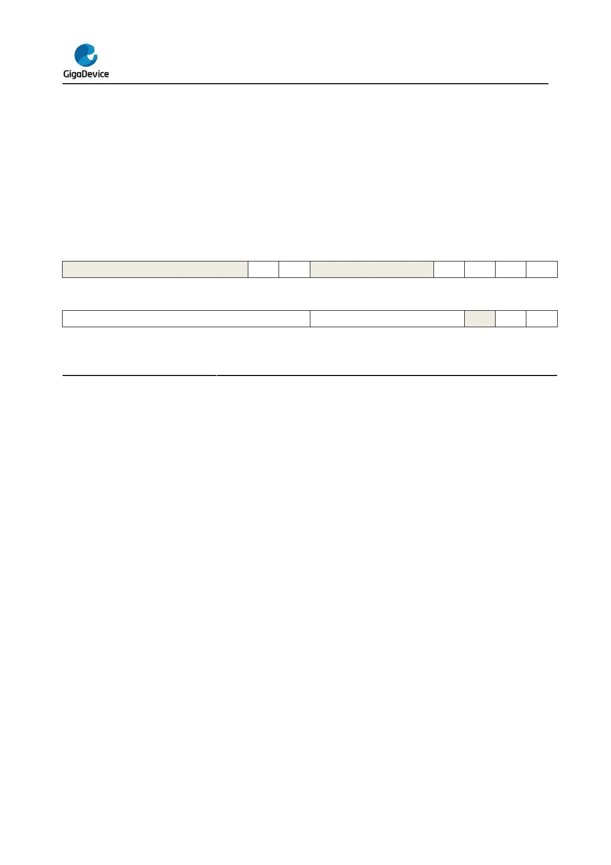
4.3.1. Control register0 (RCU_CTL0)
Address offset: 0x00
Reset value: 0x0000 XX83 where X is undefined.
This register can be accessed by byte(8-bit), half-word(16-bit) and word(32-bit)
Must be kept at reset value.
PLL Clock Stabilization Flag
Set by hardware to indicate if the PLL output clock is stable and ready for use.
0: PLL is not stable
1: PLL is stable
PLL enable
Set and reset by software. This bit cannot be reset if the PLL clock is used as the
system clock. Reset by hardware when entering Deep-sleep or Standby mode.
0: PLL is switched off
1: PLL is switched on
Must be kept at reset value.
HXTAL Clock Monitor Enable
0: Disable the External 4 ~ 32 MHz crystal oscillator (HXTAL) clock monitor
1: Enable the External 4 ~ 32 MHz crystal oscillator (HXTAL) clock monitor
When the hardware detects that the HXTAL clock is stuck at a low or high state, the
internal hardware will switch the system clock to be the internal high speed IRC8M
RC clock. The way to recover the original system clock is by either an external
reset, power on reset or clearing CKMIF by software.
Note: When the HXTAL clock monitor is enabled, the hardware will automatically
enable the IRC8M internal RC oscillator regardless of the control bit, IRC8MEN,
state.
External crystal oscillator (HXTAL) clock bypass mode enable
The HXTALBPS bit can be written only if the HXTALEN is 0.
 Loading...

