GD32F3x0 User Manual
520
full-duplex mode. In MRU or MRB mode, after SPI is enabled, the SPI continuously
generates SCK until the SPI is disabled. So the application should ignore the TBE flag and
read out reception buffer in time after the RBNE flag is set, otherwise a data overrun fault will
occur.
The slave reception mode (SRU or SRB) is similar to the reception sequence of full-duplex
mode except that the TBE bit need to be ignored.
SPI TI mode
SPI TI mode takes NSS as a special frame header flag signal and its operation sequence is
similar to normal mode described above. The modes described above (MFD, MTU, MRU,
MTB, MRB, SFD, STU, SRU, STB and SRB) are still supported in TI mode. While, in TI
mode the CKPL and CKPH bits in SPI_CTL0 registers take no effect and the SCK sample
edge is falling edge.
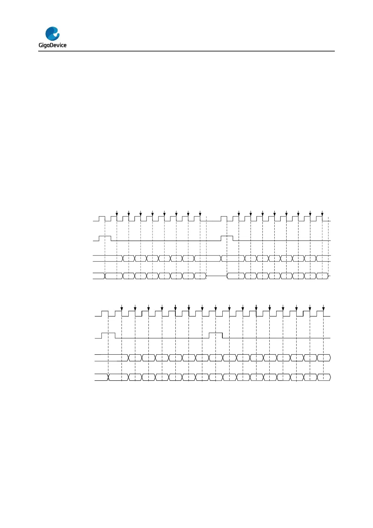
Figure 20-8. Timing diagram of TI master mode with discontinuous transfer
In master TI mode, SPI can perform continuous or non-continuous transfer. If the master
writes SPI_DATA register fast enough, the transfer is continuous, otherwise non-continuous.
In non-continuous transfer there is an extra header clock cycle before each byte. While in
continuous transfer, the extra header clock cycle only exists before the first byte and the
following bytes’ header clock is overlaid at the last bit of pervious bytes.
 Loading...

