GD32F3x0 User Manual
534
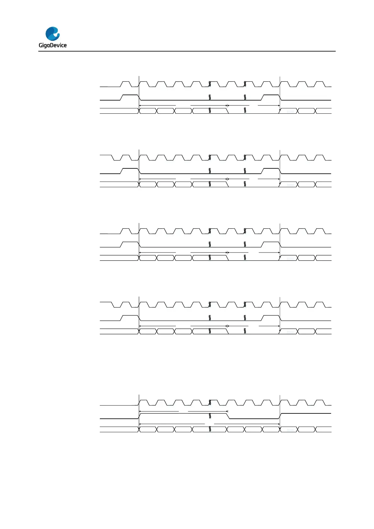
Figure 20-39. PCM standard short frame synchronization mode timing diagram
(DTLEN=01, CHLEN=1, CKPL=0)
I2S_CK
I2S_SD
24-bit data
MSB
I2S_WS
MSB
frame 1 frame 2
8-bit 0
Figure20-40. PCM standard short frame synchronization mode timing diagram
(DTLEN=01, CHLEN=1, CKPL=1)
I2S_CK
I2S_SD
24-bit data
MSB
I2S_WS
MSB
frame 1 frame 2
8-bit 0
Figure 20-41. PCM standard short frame synchronization mode timing diagram
(DTLEN=00, CHLEN=1, CKPL=0)
I2S_CK
I2S_SD
16-bit data
MSB
I2S_WS
MSB
frame 1 frame 2
16-bit 0
Figure 20-42. PCM standard short frame synchronization mode timing diagram
(DTLEN=00, CHLEN=1, CKPL=1)
I2S_CK
I2S_SD
16-bit data
MSB
I2S_WS
MSB
frame 1 frame 2
16-bit 0
The timing diagrams for each configuration of the long frame synchronization mode are
shown below.
Figure 20-43. PCM standard long frame synchronization mode timing diagram
(DTLEN=00, CHLEN=0, CKPL=0)
I2S_CK
I2S_SD
16 bits
MSB
I2S_WS
MSB LSB
frame 1 frame 2
13 bits
 Loading...

